Semiconductor Precision CNC Machining & Ultra-Clean Component Manufacturing
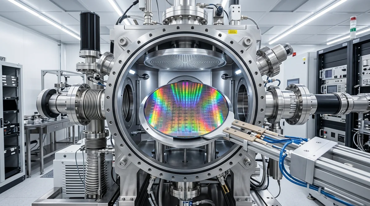
AS Prototypes provides contamination-critical precision CNC machining, Swiss micro-turning, and ultra-high vacuum (UHV) cleanroom finishing for semiconductor equipment manufacturers. From precision micro-orifice gas showerheads and wafer end-effectors to high-purity fluidic manifolds, our in-house facility turns complex geometries into production-ready hardware with precision-machined tolerances down to ±0.010 mm.
4-Stage Semiconductor New Product Introduction (NPI) Lifecycle
Bringing high-vacuum and wafer-contact mechanisms from initial CAD concepts to production requires rigorous phase-gate discipline. Our 4-stage NPI framework minimizes design risks, validates vacuum integrity, and ensures high-precision batch repeatability.
In-depth engineering review addressing virtual leak entrapment, knife-edge seal clearances, O-ring gland compression ratios, and thin-wall deflection risks under plasma etching thermal loads.
- Vacuum outgassing assessment
- Blind hole venting & slot optimization
- Tooling clearance & 5-axis collision checks
- Complete DFM feedback report
Single-setup 5-axis CNC machining of proof-of-concept parts. Verifies wafer interface coplanarity, micro-orifice flow dynamics, and initial vacuum envelope integrity before committing to tooling.
- 1 to 5 units physical prototypes
- Zeiss CMM coordinate metrology report
- Initial helium mass spec leak test
- Raw material mill test reports (MTR)
Low-volume pilot production batch (10 to 100 pcs). Validates electropolishing passivation bath chemistry, anodizing coating thickness consistency, and cleanroom ultrasonic particulate removal protocols.
- 10 to 100 pcs pilot batch run
- First Article Inspection (FAI) documentation
- Surface profilometry validation (Ra ≤ 0.2 μm)
- Double-sealed cleanroom packaging
Scaled multi-axis production with strict Copy-Exact process baselines. Locked CNC programs, dedicated tooling suites, and batch-level Statistical Process Control (SPC) for global fab equipment deployments.
- 100 to 1,000+ units on scheduled releases
- Locked CAM toolpaths & raw material lots
- Continuous CPK / PPK metrology tracking
- Dedicated safety stock & buffer warehousing
Core Precision Capabilities for Semiconductor Applications
Machining components for high-vacuum, wafer handling, and corrosive gas delivery requires specialized manufacturing processes capable of holding tight dimensional tolerances down to ±0.005 mm while eliminating micro-burrs and surface defects.
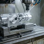
Machining complex 3D monolithic structures, vacuum chamber lids, wafer chuck bodies, and fluidic distribution manifolds in a single setup, eliminating cumulative datum stacking errors.
Machining Tolerance: ISO 2768-mK (±0.05 mm envelope; ±0.010 mm critical bores)
Typical Materials: Al 6061-T6, Al 7075-T651, SS 316L VIM/VAR
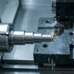
Specialized multi-axis sliding-headstock turning for micro fluidic fittings, high-frequency pogo pins, sensor nozzles, and optical guide shafts with mirror-like surface finishes.
Runout & Diametrical Tol: ±0.005 mm on metals; ±0.020 mm on polymers
Typical Materials: 316L, Beryllium Copper, Torlon 4203
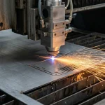
Stress-free electrical discharge machining for micro-apertures, narrow gas-dispersion slots, and sharp internal 90° corners without mechanical cutter deflection.
Internal Corner Radius: R < 0.03 mm
Typical Materials: Tungsten, Molybdenum, Inconel 718, SS 316L, Titanium Gr. 5
Electropolishing (Ra ≤ 0.1 μm), ASTM A967 chemical passivation, and hard anodizing combined with multi-stage ultrasonic degreasing to achieve ultra-low outgassing compliant with UHV standards.
Cleaning Protocols: DI water rinse + Class 100 vacuum seal
Standards: ASTM B912, ASTM A967, MIL-A-8625
Semiconductor Component Showcase Cards
Engineered components built for lithography scanners, etch reactors, chemical mechanical planarization (CMP), and IC testing systems. Each part is matched to its optimal manufacturing process with transparent DFM tolerance tiers.
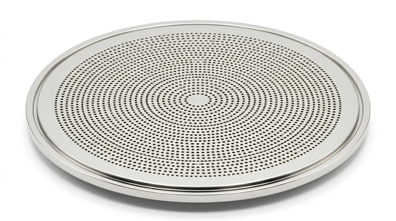
Gas Distribution Showerhead Plates
3-Axis Micro-DrillPlanar showerheads containing thousands of precision micro-apertures designed to distribute precursor and etch gases across silicon wafers. Executed on 30,000 RPM micro-drilling spindles to avoid costly 5-axis overhead.
Cost-Effective Tolerance: ISO 2768-m (±0.1 mm) on outer disc diameter
Critical Fit Tolerance: ±0.015 mm Orifice Diameters; 0.02 mm Face Flatness
Recommended Materials: Al 6061-T651 (High Purity), Stainless Steel 316L VIM/VAR, Nickel 200.
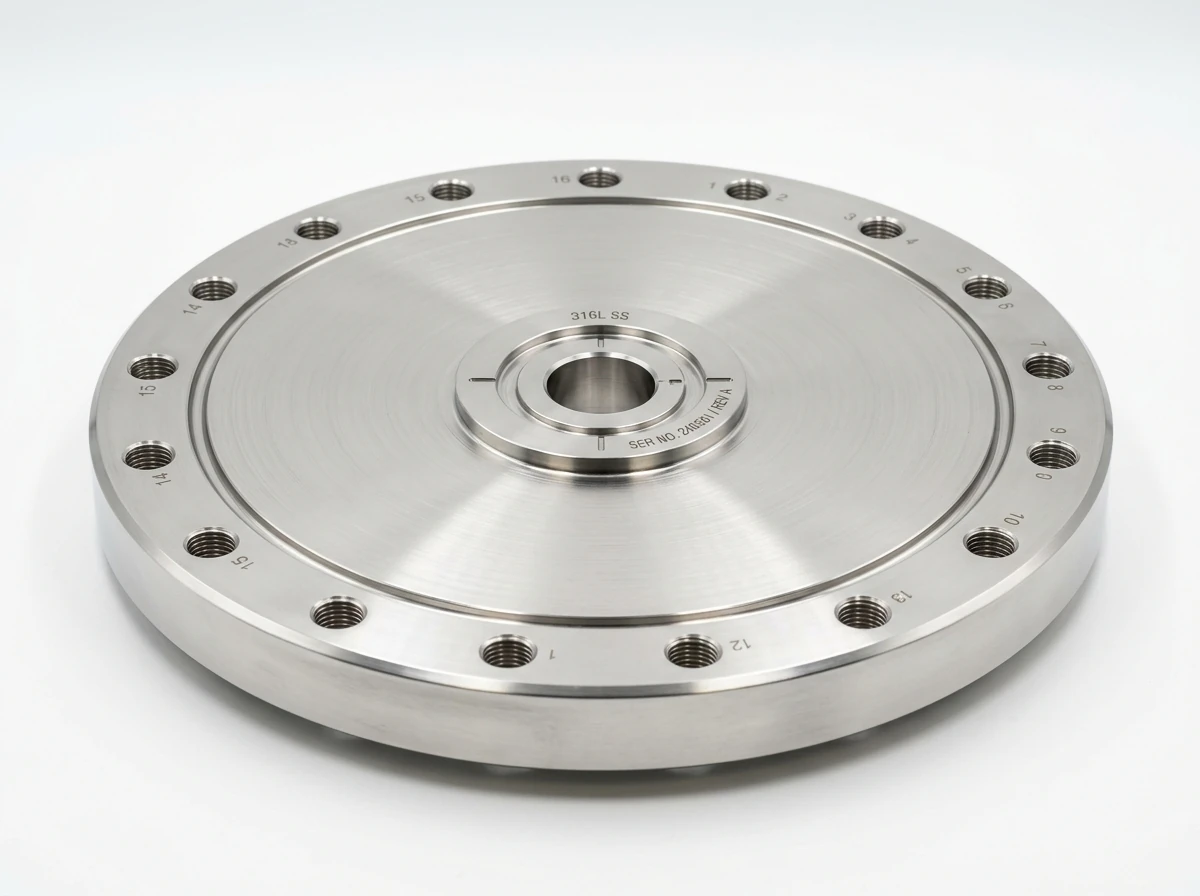
UHV Chamber Lids & ConFlat (CF) Flanges
3-Axis MillingHeavy-duty vacuum chamber access covers and ConFlat flanges engineered to maintain ultra-high vacuum (< 10⁻⁹ Torr) under thermal cycling during epitaxial growth and ALD processes.
Cost-Effective Tolerance: ISO 2768-m (±0.1 mm) Flange Envelope & Bolt Circle
Critical Fit Tolerance: ±0.010 mm CF Knife-Edge Profile (Ra ≤ 0.4 μm)
Recommended Materials: SS 316L-ESR (Forged), SS 316L VIM/VAR, Al 6061-T651.
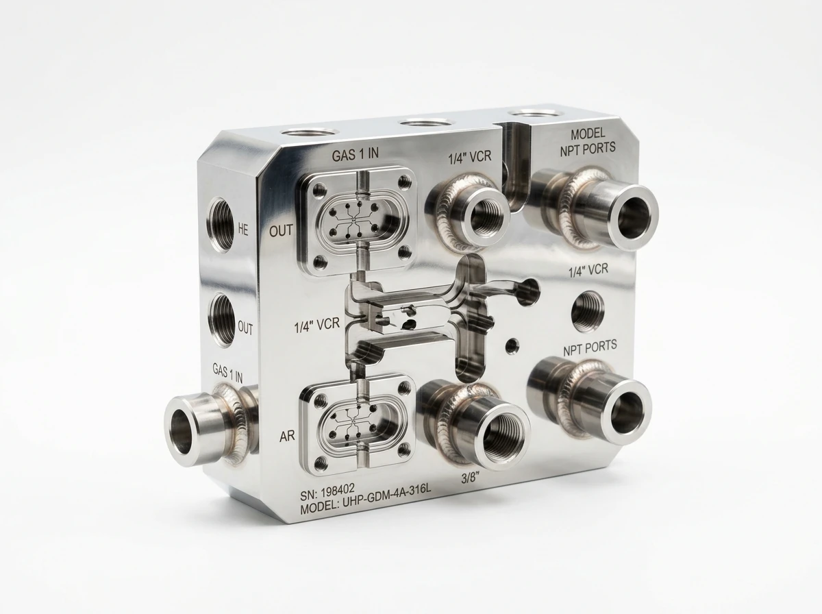
Mass Flow Controller (MFC) Manifolds
4-Axis Index MillingMonolithic multi-channel gas distribution blocks routing hazardous, pyrophoric, and precursor gases without external fittings. 4-axis indexing enables single-setup cross-drilled internal channels.
Cost-Effective Tolerance: ISO 2768-m (±0.1 mm) Block Exterior Dimensions
Critical Fit Tolerance: ±0.015 mm Port Alignment; 0.015 mm Seal Face Flatness
Recommended Materials: 316L VIM-VAR Double Melt, Hastelloy C-22.
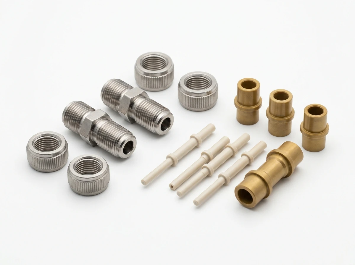
Micro Gas Fittings & PEEK Guide Pins
Swiss TurningSlender VCR/CF face-seal gland fittings, micro-metering orifices, and virgin Torlon/PEEK precision isolator guide pins for IC test sockets. Swiss lathes eliminate slender-part deflection.
Cost-Effective Tolerance: ISO 2768-m (±0.08 mm) Overall Length & Flanges
Critical Fit Tolerance: ISO h6/h7 (±0.008 mm) Fitting Diameters & Micro Pins
Recommended Materials: 316L SS, Virgin PEEK, Torlon 4203.
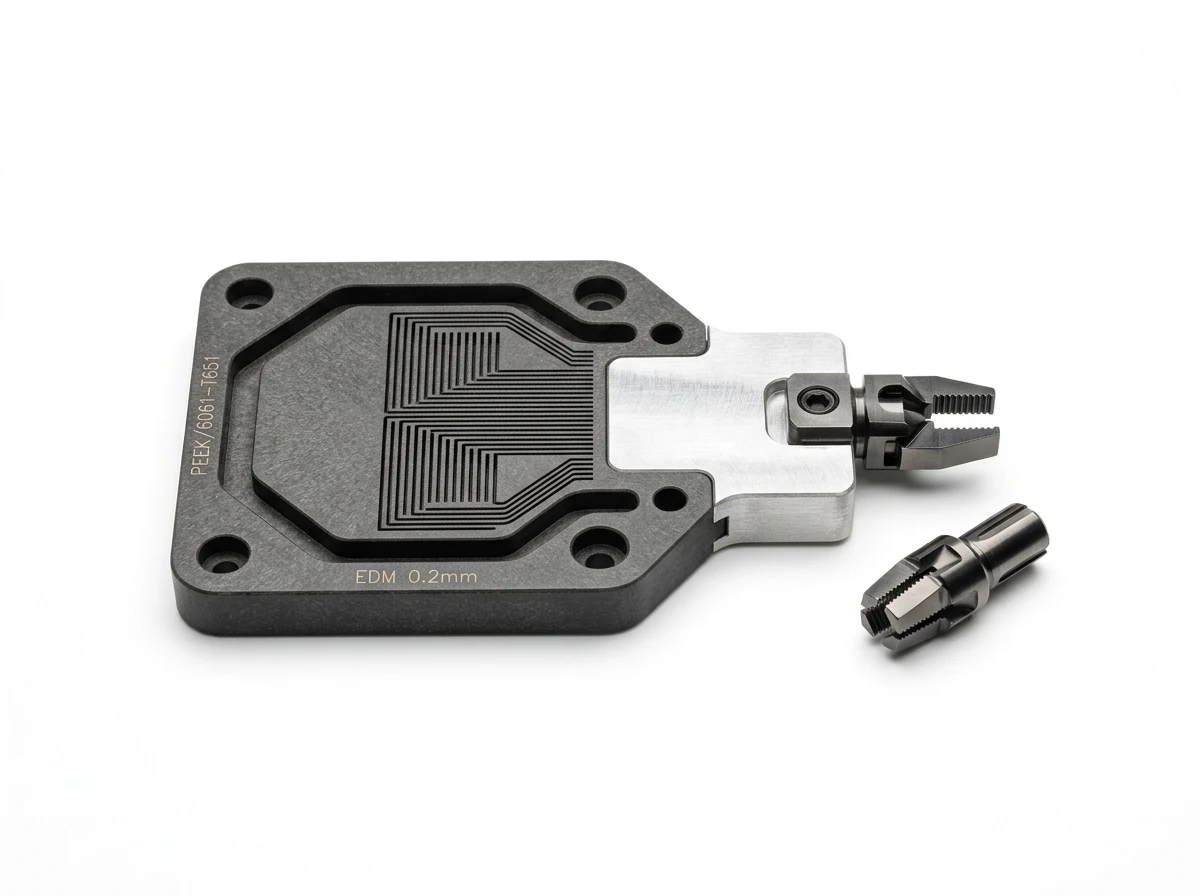
Wafer End-Effectors & Tungsten Collets
Wire EDMRobotic wafer transfer paddles with internal 0.2mm vacuum suction slits, micro-gripping collets, and flexure joints. Wire EDM vaporizes metal without mechanical cutting forces, preventing thin-arm deflection.
Cost-Effective Tolerance: 3-Axis Pre-Mill ISO 2768-m for arm contour
Critical Fit Tolerance: ±0.005 mm Wire Cut Slits; R ≤ 0.05 mm Corners
Recommended Materials: Ceramic-Filled PEEK, 6061-T651, Tungsten Carbide.
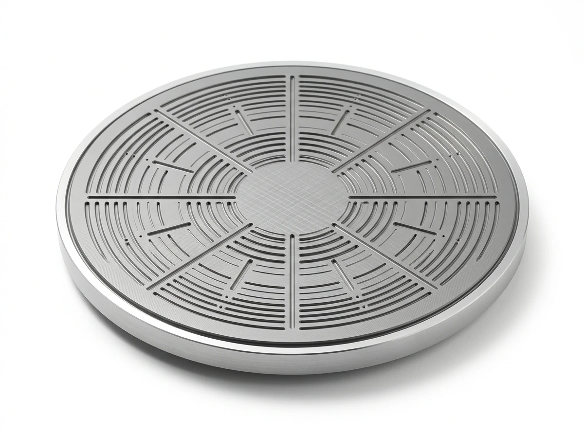
Electrostatic Chucks (ESC) & Pedestals
Precision Grinding300mm wafer pedestals with helium backside cooling channels and ceramic dielectric surfaces. Precision horizontal rotary surface grinders achieve 0.005 mm ground coplanarity across the entire 300 mm chuck surface.
Cost-Effective Tolerance: ISO 2768-m (±0.08 mm) External Rim & Ports
Critical Fit Tolerance: 0.005 mm Ground Flatness Across 300 mm Span
Recommended Materials: High-Purity Aluminum, Silicon Carbide, Invar 36.
Semiconductor Materials & Precision CNC Parameter Matrix
Comprehensive material selection matrix detailing vacuum compatibility, outgassing limits, machining tolerances, and surface roughness capabilities across primary semiconductor alloys, ceramics, and advanced polymers.
| Material Designation | Alloy / Class Spec | Vacuum & Outgassing (TML / CVCM) | Precision CNC Tolerance | Achievable Surface Finish | Primary Semiconductor Applications |
|---|---|---|---|---|---|
| Aluminum 6061-T6 / 7075-T651 | High-Purity wrought Al alloy | TML < 0.05% | CVCM < 0.01% (UHV Compatible) | ±0.008 mm | Ra 0.2 μm (Milled / Turned) | Vacuum chamber bodies, wafer handling arms, stage brackets, showerhead plates. |
| Stainless Steel 316L VIM/VAR | Vacuum Induction / Arc Remelt | Ultra-Low Outgassing | Minimal non-metallic inclusions (VIM-VAR melt quality) | ±0.005 mm | Ra 0.1 μm (Electropolished) | MFC gas delivery blocks, UHV CF flanges, corrosive chemical supply lines. |
| Titanium Grade 5 (Ti-6Al-4V) | Alpha-Beta Titanium Alloy | Non-Magnetic | Extreme chemical stability | ±0.008 mm | Ra 0.4 μm (Precision ground) | Wafer clamp rings, high-stress load lock structural components, heater mounts. |
| Torlon 4203 / 5530 (PAI) | Polyamide-Imide (Unfilled / 30% Glass) | Low Outgassing | HDT 278°C | Low CTE | ±0.008 mm | Ra 0.4 μm (Diamond micro-tooled) | Fine-pitch IC test sockets, burn-in nests, wafer probe card positioning blocks. |
| Semiconductor PEEK (Virgin / ESD) | Polyetheretherketone (High Purity) | TML < 0.15% | High plasma resistance | ±0.010 mm | Ra 0.4 μm (Precision turned) | CMP retaining rings, wafer cassette guides, wet bench chemical valve seats. |
| Macor Machinable Glass-Ceramic | Zero-porosity fluorophlogopite mica | Ultra-low outgassing (TML < 0.01%) | Stable up to 800°C continuous | ±0.005 mm | Ra 0.2 μm (Polished) | High-voltage feedthrough insulators, ion implanter spacers, sensor holders. |
| Optical Quartz / Fused Silica | 99.99% SiO2 High-Purity Quartz | Ultra-low outgassing (TML < 0.01%) | Near-zero thermal expansion | ±0.005 mm (Ultrasonic/Grind) | Optical Ra 0.05 μm | Plasma chamber optical viewports, wafer support boats, pyrometer sight glass. |
Quality Assurance & Cleanroom Metrology Protocol
Every semiconductor component machined at AS Prototypes is subjected to rigorous dimensional validation, vacuum integrity verification, and multi-stage ultrasonic cleanroom preparation before dispatch.
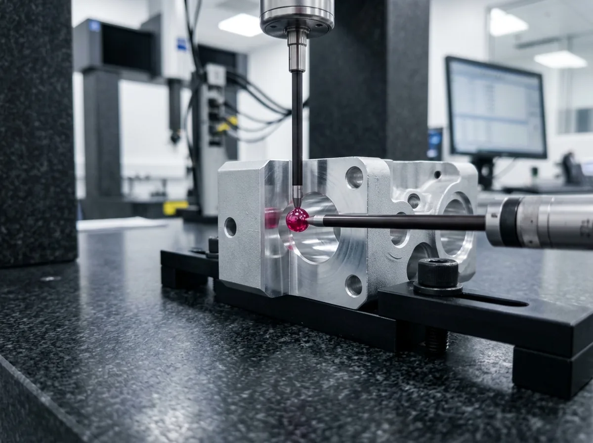
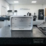
Zeiss CMM Spatial Metrology
High-precision 3D coordinate scanning verifying hole pitches, knife-edge seal profiles, true positions, and geometric profile tolerances (GD&T) against native engineering CAD models.
Helium Mass Spectrometry
Calibrated sniffing and vacuum-hood helium leak testing capable of detecting leak rates down to < 1×10⁻¹⁰ mbar·l/s, verifying hermetic sealing down to < 1×10⁻¹⁰ mbar·l/s for high-reliability UHV performance.
Optical Surface Profilometry
Non-contact white-light optical profilometry verifying surface roughness parameters (Ra, Rz, Rmax) on electropolished gas wetted pathways down to Ra 0.1 μm without scratch risks.
Cleanroom Ultrasonic Decontamination
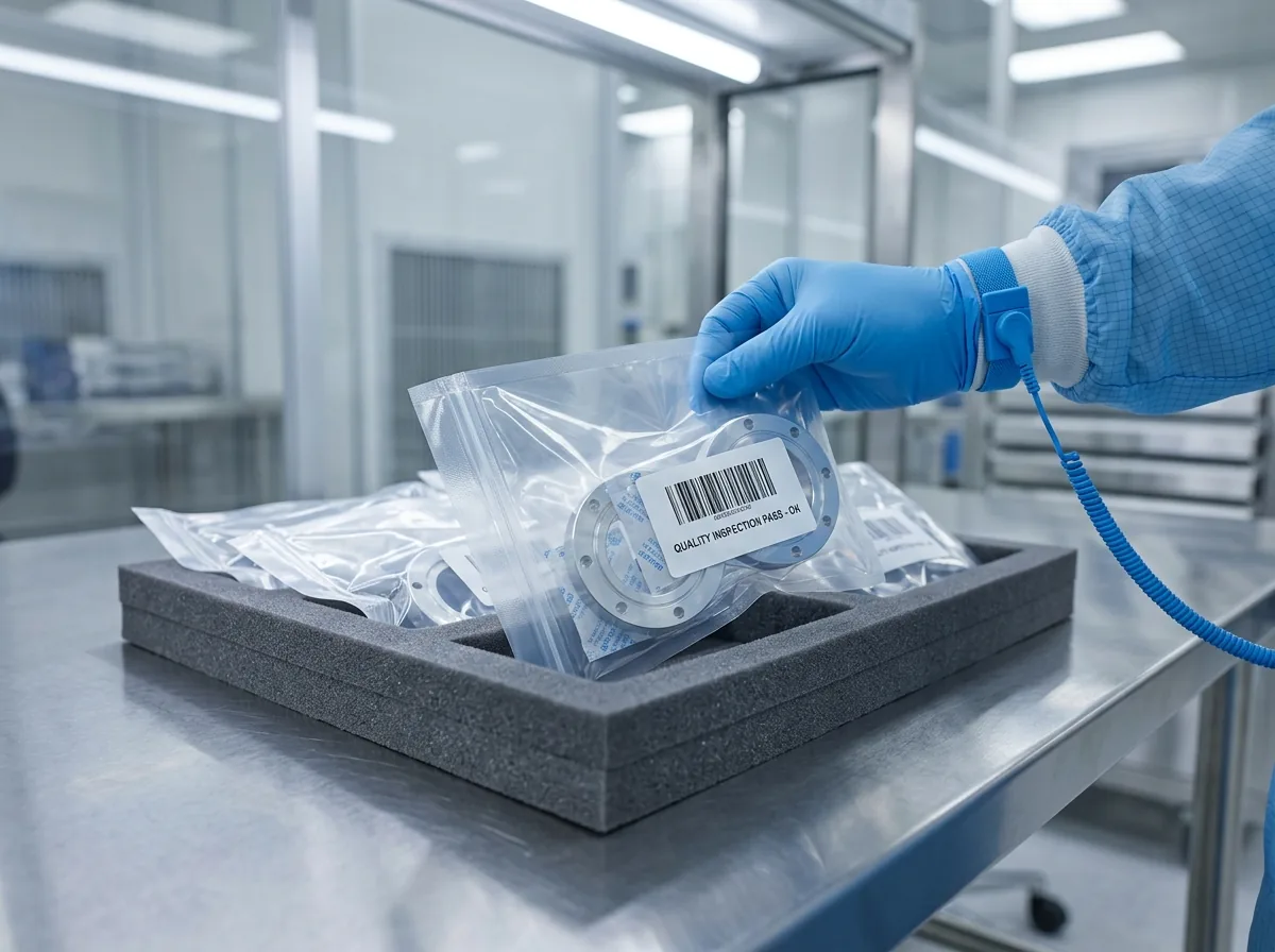
Multi-frequency ultrasonic baths with semiconductor-grade surfactants and DI water cascade rinses, followed by nitrogen drying and double-sealed vacuum bagging inside Class 100 cleanrooms.
Frequently Asked Questions: Semiconductor Precision Machining
Key technical considerations regarding vacuum outgassing, material selection, helium leak testing, and cleanroom packaging for semiconductor fabrication components.
Virtual leaks occur when gas is trapped inside blind tapped holes, micro-cracks, or porous raw material pockets. We eliminate virtual leaks by implementing vented screws or CNC machining longitudinal venting slots in internal threaded holes, maintaining generous internal corner radii, sourcing exclusively forged or vacuum-arc remelted metals (such as 316L-ESR and VIM/VAR), and delivering surface electropolishing (Ra ≤ 0.1 μm) to remove microscopic crevices where atmospheric moisture could linger.
Standard commercial 316L stainless steel contains non-metallic microscopic oxide and sulfide inclusions that corrode when exposed to aggressive semiconductor etching gases like Cl2, BCl3, and HBr. 316L VIM/VAR undergoes double melting—Vacuum Induction Melting followed by Vacuum Arc Remelting—resulting in an exceptionally pure grain structure, ultra-low sulfur content, zero micro-voids, and superior passivity under high-purity electropolishing.
Yes. Utilizing specialized high-speed CNC drilling spindles (up to 30,000 RPM), custom micro-grain carbide drills, and advanced Wire EDM, we routinely drill arrays of over 5,000 micro-orifices (Ø0.3 mm to Ø0.5 mm) across Ø300 mm showerhead plates. Our multi-axis toolpaths ensure zero entry and exit burrs, hole diameter consistency within ±0.010 mm, with burr-free entry/exit and smooth flow pathways (Ra ≤ 0.8 μm as-drilled; Ra ≤ 0.4 μm with chemical polishing).
Following machining and deburring, components undergo multi-stage ultrasonic degreasing in semiconductor-grade aqueous detergent baths, followed by multi-stage deionized (DI) water cascade rinsing (resistivity > 18 MΩ·cm). Cleaned parts are baked in clean vacuum ovens to drive out residual moisture and outgassing volatiles, then double-bagged and vacuum-sealed in anti-static, nitrogen-purged poly bags within our Class 100/1000 cleanroom.
For rapid engineering prototypes (1–5 pcs), our standard ex-factory turnaround is 4 to 8 business days (simple parts without complex finishes). Components requiring electropolishing, ASTM A967 passivation, or hard anodizing are delivered within 7 to 12 business days. Pilot and low-volume production batches (10–100+ pcs) require 7 to 30 business days depending on geometric complexity and material availability. International express air transit via DHL or FedEx requires an additional 3 to 5 business days.