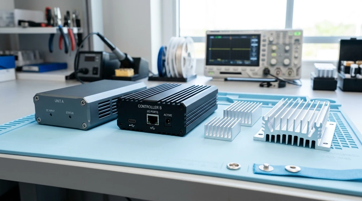
Modern electronic hardware engineering demands enclosures and chassis that serve far beyond simple protective packaging. In high-performance electronic devices, an aluminum chassis operates simultaneously as an EMI containment vessel, a structural heatsink, a dielectric insulator, and a precision-toleranced mechanical backbone. Electrochemical anodizing converts the raw aluminum substrate into an engineered ceramic-like anodic oxide barrier, fundamentally resolving the operational conflicts between heat dissipation, electrical short circuits, and harsh environmental wear.
Quick Engineering Takeaways (BLUF)
- Dielectric Isolation: MIL-A-8625 Type II (15–25 μm) provides 500–1,000 V breakdown resistance; Type III Hardcoat (40–50 μm) delivers 1,500–2,500 V standoff, eliminating accidental chassis shorts and high-voltage PCB arcing.
- Radiative Thermal Emissivity: Bare machined aluminum exhibits a low thermal emissivity (ε ≈ 0.04–0.08), reflecting heat back inward. Black anodizing elevates emissivity to ε ≈ 0.90–0.94, increasing total passive heat dissipation by roughly 15% to 30% in fanless enclosures, depending on fin geometry.
- EMI Grounding & Selective Masking: Anodic alumina is non-conductive. Maintaining Faraday cage continuity requires high-precision silicone masking or secondary CNC spot-facing on grounding bosses, keeping contact resistance below 0.05 Ω.
- Dimensional Growth & Thread DFM: Anodizing follows the 50/50 penetration-growth rule. Critical bearing bores shrink by the total coating thickness, and 60° thread pitch diameters shift by approximately 4× growth, requiring pre-anodize oversize taps (6G/GH3) or silicone thread plugs.
- Surface Durability: Dense nickel acetate sealing converts micro-porous alumina into hydrated pseudo-boehmite, meeting the 336-hour MIL-A-8625 ASTM B117 neutral salt spray requirement (500+ hours achievable) and resisting skin sebum pitting.
1. Electrochemical Alumina Synthesis: Turning Metal into Ceramic
When exposed to ambient air, bare aluminum naturally develops a thin native oxide film approximately 2 to 4 nanometers thick. While this spontaneous passivation layer prevents immediate atmospheric corrosion, it lacks the physical density, structural thickness, and mechanical hardness required for industrial electronics. Electrochemical anodizing accelerates and amplifies this natural oxidation inside a temperature-controlled acid electrolyte bath (typically 15% to 20% sulfuric acid by weight, H2SO4) under regulated direct current.
Under applied electrical potential, the aluminum workpiece functions as the anode. Water molecules in the aqueous bath dissociate, releasing nascent oxygen ions (O2−) that migrate toward the anode surface to react with aluminum ions (Al3+). The overall electrochemical conversion follows the stoichiometric formula:
2 Al + 3 H2O → Al2O3 + 6 H+ + 6 e−
Simultaneously, the acidic electrolyte chemically dissolves a minute fraction of the newly synthesized alumina. The equilibrium between electrochemical growth and acidic dissolution produces a unique self-organizing microscopic architecture: a thin, pore-free barrier layer (10 to 30 nm thick) adjacent to the bare metal, capped by a dense columnar hexagonal cell matrix containing microscopic vertical pores (10 to 25 nm in diameter). This cellular structure forms the physical foundation for the electrical, thermal, and optical properties that make anodizing essential for modern electronics.
| Finishing Specification | Coating Thickness | Dielectric Breakdown Voltage | Thermal Emissivity (ε) | Hardness / Wear Resistance | Primary Electronic Applications |
|---|---|---|---|---|---|
| MIL-A-8625 Type II Class 1 (Clear Sulfuric) | 10 – 25 μm | 500 – 1,000 V | 0.82 – 0.86 | 250 – 350 HV | Internal chassis trays, RF cavity dividers, front bezel plates |
| MIL-A-8625 Type II Class 2 (Dyed Black / Colored) | 15 – 25 μm | 500 – 1,000 V | 0.90 – 0.94 | 250 – 350 HV | Consumer device enclosures, handheld housings, passive cooling frames |
| MIL-A-8625 Type III Class 1/2 (Hardcoat) | 35 – 65 μm | 1,500 – 2,500 V | 0.86 – 0.92 | 400 – 550 HV | Rugged industrial tablet frames, military telemetry units, field gear |
| MIL-DTL-5541 Type II Class 3 (Chem Film / Alodine) | 0.1 – 0.5 μm | 0 V (Electrically Conductive) | 0.15 – 0.22 | Substrate Hardness | Chassis grounding pads, RF gasket lands, PCB mounting bosses |
2. Dielectric Isolation: High-Voltage Breakdown & PCB Arc Prevention
One of the most consequential functional improvements anodizing brings to electronic products is electrical insulation. Pure alumina (Al2O3) is an exceptional dielectric ceramic material with a volume resistivity exceeding 1014 Ω·cm at room temperature. In contrast, bare raw aluminum has an extremely low volume resistivity of 2.82 × 10⁻⁶ Ω·cm, meaning uninsulated contact with an energized circuit creates an instantaneous low-resistance short circuit.
In compact electronic assemblies—such as compact power supplies, motor controllers, drone flight controllers, and edge computing servers—surface-mount PCB components and tall electrolytic capacitors sit within fractions of a millimeter from the metal enclosure. Mechanical vibration, thermal expansion, or dropping impact can flex the circuit board, driving energized traces into contact with the housing walls. An anodized barrier effectively isolates up to 1,000 volts DC on standard Type II coatings and upwards of 2,000 volts on Type III hardcoat layers, reducing the risk of hazardous electrical flashover.
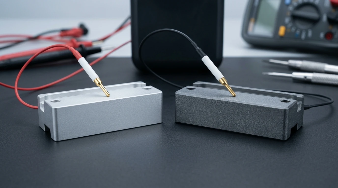
Furthermore, electronic enclosures must withstand severe Electrostatic Discharge (ESD) transients. According to IEC 61000-4-2 standards, consumer and industrial hardware must endure up to 8 kV contact discharge and 15 kV air discharge. An anodized outer skin acts as a protective dielectric shield, preventing electrostatic charge from arcing directly into internal sensitive silicon microchips, analog sensors, and high-speed data buses. Designers must account for the dielectric constant (εr ≈ 8.5 to 9.5) and dissipation factor of alumina when designing high-frequency RF modules to avoid unwanted parasitic capacitance.
3. Thermal Radiation Physics: Maximizing Passive Heat Dissipation
A widespread misconception among junior mechanical engineers is that anodizing impedes heat transfer because alumina has a lower bulk thermal conductivity (20 to 30 W/m·K) than raw 6061-T6 aluminum (167 W/m·K). However, conductive thermal resistance is directly proportional to thickness: Rcond = t / (k · A). Because an electronic anodized film is only 15 to 25 micrometers thick, its conductive thermal resistance is practically negligible (typically well under 0.01 K/W over a 25 cm² contact area), producing a negligible thermal penalty at the component interface.
Conversely, anodizing introduces a massive thermal advantage in radiative heat transfer. Heat dissipation in electronic systems occurs via three simultaneous mechanisms: conduction, convection, and radiation. In sealed, fanless enclosures (such as IP67 outdoor 5G radios, hazardous area telemetry units, and automotive sensor pods), internal air velocity is near zero, meaning natural convection is limited. Under these conditions, thermal radiation typically accounts for roughly 20% to 35% of total dissipated heat flux, depending on fin geometry and exposed surface area.
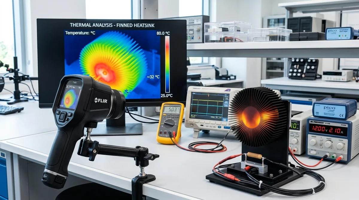
Radiative thermal power is governed by the Stefan-Boltzmann law:
q = ε · σ · A · (Tsurface4 − Tambient4)
Where σ is the Stefan-Boltzmann constant (5.670 × 10⁻⁸ W/m2·K4), A is surface area, and ε is the surface emissivity coefficient. Highly polished or bare machined aluminum is an outstanding thermal reflector and an exceptionally poor radiator, with an emissivity coefficient of only ε ≈ 0.04 to 0.08. It reflects over 92% of infrared heat waves back into the enclosure core. Anodizing converts the surface into a near-ideal infrared blackbody radiator. Even clear anodizing elevates ε to 0.82–0.86, while matte black anodizing achieves ε ≈ 0.90–0.94. This radiant boost lowers junction temperatures on high-power microprocessors by roughly 3°C to 10°C under identical passive operating conditions, depending on fin geometry and power density.
| Surface Finish Condition | Thermal Emissivity (ε) | Indicative Radiated Heat Share (Fanless, Finned) | Thermal Performance Index | Common Hardware Use Case |
|---|---|---|---|---|
| Bare CNC Milled 6061-T6 (Raw) | 0.04 – 0.08 | 3% – 8% | Baseline (Poor Radiator) | Internal structural brackets, internal battery trays |
| Glass Bead Blasted Bare Aluminum | 0.18 – 0.25 | 8% – 15% | Slight Improvement | Non-cosmetic unsealed prototypes |
| Clear Anodized Type II (15 μm) | 0.82 – 0.86 | 20% – 30% | High Performance | Silver laptop shells, natural telecom chassis |
| Black Anodized Type II/III (25 μm) | 0.90 – 0.94 | 25% – 35% | Maximum Passive Cooling | Microprocessor heatsinks, LED spotlights, audio amplifiers |
| MIL-DTL-5541 Chem Film (Gold/Clear) | 0.15 – 0.22 | 5% – 10% | Low Radiation / High Conduction | Internal RF shield walls, PCB ground interfaces |
4. Solving the Dielectric Paradox: EMI Grounding & Selective Masking
While the non-conductive nature of an anodized surface provides invaluable dielectric isolation, it introduces an engineering dilemma: electronic hardware requires continuous electrical conductivity across enclosure seams to create an effective Faraday cage. Without metallic continuity, electromagnetic interference (EMI) leaks out of the device, failing FCC and CE compliance testing. Furthermore, internal printed circuit boards require low-impedance ground bonding paths (typically < 0.05 Ω) to safely sink return currents and electrostatic charges.
To resolve this dielectric conflict, AS Prototypes deploys three proven engineering strategies during manufacturing:
1. Precision Selective Masking: Prior to immersion in the anodizing tanks, skilled technicians apply specialized high-temperature silicone rubber plugs into threaded blind holes, or place custom die-cut vinyl and polyimide (Kapton) masking tapes over flat PCB grounding bosses. During the electrochemical cycle, the electrolyte cannot touch the masked regions. After stripping the masks, pristine raw aluminum remains on the grounding lands, ready for low-resistance electrical contact.
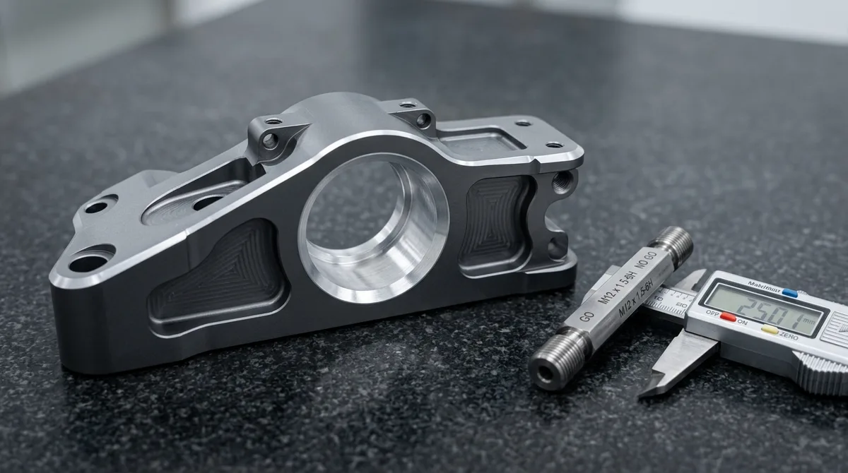
2. Post-Anodize Secondary CNC Machining: For complex RF cavity enclosures requiring sub-millimeter grounding perimeters or conductive gasket tracks, parts undergo full Type II or Type III anodizing first. The anodized enclosure is then loaded back onto our high-speed 3-axis or 4-axis CNC milling centers. A secondary spot-facing or engraving pass cuts away 0.05 mm of the anodic skin, exposing mirror-smooth conductive aluminum tracks. This method eliminates human masking misalignment and helps minimize EMI leakage.
3. Dual-Finish Conversion Coating: In mission-critical aerospace and communications modules, exposed raw aluminum on unanodized grounding pads could suffer galvanic corrosion over time. We apply a dual-process sequence: full anodizing on cosmetic exterior faces, followed by targeted application of MIL-DTL-5541 Type II Class 3 clear chemical conversion film (chem film) across grounding pads. Chem film provides corrosion resistance while maintaining low surface contact resistance (< 5 mΩ/in2).
5. Precision Dimensional Growth, Tolerance Budgets & Thread DFM
Unlike wet spray painting or electroplating—which purely add material onto the external substrate—anodizing is an electrochemical conversion process governed by the 50/50 rule. Approximately 50% of the anodic film thickness penetrates into the core aluminum alloy, while the remaining 50% builds outward beyond the original machined surface boundary. Understanding this dimensional shift is critical when tolerancing tight-tolerance dowel pin bores, bearing press-fits, and fine-pitch threads.
For a standard Type II coating of 20 μm total thickness, external dimensions expand by 10 μm per side (+20 μm on overall outside diameter or thickness). Simultaneously, internal holes and bores shrink by 10 μm per side (−20 μm on inside diameter). For Type III hardcoat anodizing (50 μm total thickness), outward growth is 25 μm per side. A precision H7 bearing bore (e.g., +0.021/0 mm on Ø20) will close by 0.050 mm if left unmasked, resulting in complete assembly failure.
Dimensional growth impacts internal 60° metric and Unified screw threads even more severely. Because thread flanks are inclined at 30° to the radial plane (60° included angle), outward growth on both flanks creates a geometrical pitch diameter shift approximately four times the outward growth:
ΔPD ≈ 4 × tgrowth ≈ 2 × tcoating
A 25 μm hardcoat thickness causes a 50 μm pitch diameter reduction, which easily jams standard 6H or 2B thread Go-gauges. In our CNC machine shop, machinists compensate for this growth during pre-plating milling by selecting oversize taps (such as 6G or GH3 tolerance classes) or utilizing helical thread milling with CAM offsets, to help thread gauges pass after anodizing.
| Feature / Dimension Type | Pre-Anodize CNC Target | Total Coating (Type II, 20 μm) | Total Coating (Type III, 50 μm) | AS Prototypes DFM Recommendation |
|---|---|---|---|---|
| Outer Width / Thickness (OD) | Nominal − 0.020 mm | +0.020 mm (+0.010 mm/side) | +0.050 mm (+0.025 mm/side) | Program CAM toolpaths to lower limit of ISO 2768-mK |
| Internal Precision Bore (ID) | Nominal + 0.020 mm | −0.020 mm (−0.010 mm/side) | −0.050 mm (−0.025 mm/side) | Mask critical bearing bores (≤ ±0.012 mm) with silicone plugs |
| Metric Internal Threads (M2 to M6) | Oversize 6G Tap Pitch | −0.040 mm on Pitch Dia | −0.100 mm on Pitch Dia | Use 6G/GH oversize taps or mask holes smaller than M3 |
| External Sharp Corners | R ≥ 0.50 mm Edge Radius | Edge thinning ≈ 5 μm | Edge burning / soft oxide risk | Break sharp corners with 0.5 mm × 45° chamfer to prevent flaking |
| Deep Blind Pockets (> 5× depth) | R ≥ 1.5 mm Floor Radii | Uniform throw | Electrolyte entrapment risk | Add ∅1.5 mm acid drainage and air-bleed holes to blind features |
6. Sealing Metallurgy: Hydrothermal Hydration & Fingerprint Resistance
Directly following the anodizing bath, the anodic oxide coating consists of an open, honeycomb-like matrix of hexagonal nanopores. If left unsealed, these microscopic pores readily absorb atmospheric moisture, industrial oils, and human skin secretions (sebum and lactic acid), producing permanent staining, discoloration, and rapid pitting corrosion. Proper chemical sealing transforms this fragile sponge into a chemically inert, non-porous ceramic armor.
The sealing process relies on hydrothermal hydration. Immersing the anodized parts in deionized water heated to 96°C to 100°C reacts the amorphous aluminum oxide walls into crystalline pseudo-boehmite (AlO(OH)):
Al2O3 + H2O → 2 AlO(OH)
This reaction causes a volumetric expansion of approximately 33%, physically swelling the alumina crystal lattice and sealing the central nanopores completely shut. For enhanced corrosion resistance, hot nickel acetate baths (95°C to 98°C) precipitate nickel hydroxide salts directly inside the pore necks. This locks organic dye molecules securely in place, reduces UV bleaching, and equips electronic housings to meet the 336-hour ASTM B117 neutral salt spray requirement of MIL-A-8625 (500+ hours is achievable on well-sealed films).
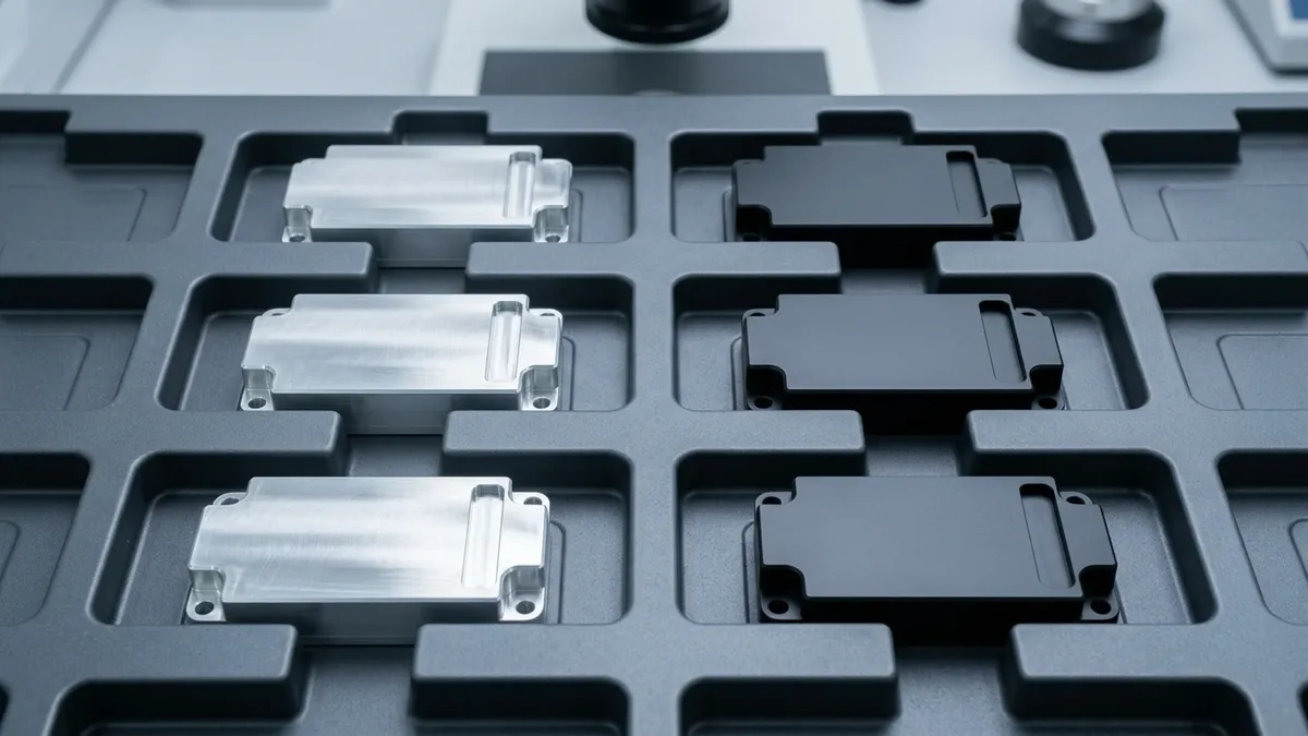
Beyond corrosion, electronic devices must resist daily mechanical handling, coin scratches, key abrasions, and desktop sliding wear. Bare 6061-T6 aluminum has a modest hardness of approximately 95 HB (105 HV), making it vulnerable to gouging. Type II anodizing increases surface hardness to 250–350 HV, while Type III hardcoat reaches 400–550 HV—comparable to hardened carbon steel. In Taber abrasion testing (CS-17 wheel, 1,000 g load), hardcoat anodized aluminum displays wear resistance comparable to hard chromium electroplating.
7. Electronic Aluminum Alloys: Grade Selection & Anodizing Response
The cosmetic uniformity, dielectric strength, and dimensional predictability of an anodized electronic part depend fundamentally on the metallurgical purity of the base aluminum alloy. Alloying elements such as silicon (Si), copper (Cu), zinc (Zn), and iron (Fe) react differently during electrochemical oxidation, altering both color and coating integrity.
Our engineering team regularly guides hardware designers across the four primary electronic alloy families:
6061-T6 / 6061-T651: The undisputed gold standard for CNC machined electronic chassis. Containing 0.8%–1.2% magnesium and 0.4%–0.8% silicon, it forms magnesium silicide (Mg2Si) precipitates that machine cleanly with minimal burrs. It takes Type II clear, dyed black, and custom color anodizing with exceptional consistency, providing uniform dielectric insulation and pristine aesthetics.
6063-T5 / 6063-T6: The preferred choice for extruded heatsinks and consumer tablet chassis. With lower iron and silicon contents, 6063 yields a clearer, brighter anodic film than 6061 and boasts higher thermal conductivity (~200 W/m·K vs 167 W/m·K), making it the premier grade for passive heat spreader profiles.
5052-H32: The primary alloy for precision sheet metal electronic housings, server racks, and folded EMI covers. High magnesium content (2.2%–2.8%) provides excellent cold-forming ductility without cracking at bend radii. It takes black anodizing superbly, though clear anodizing exhibits a subtle yellowish/matte hue compared to 6000-series alloys.
7075-T651: Deployed in high-stress aerospace telemetry, military drones, and portable medical robotics where extreme specific strength is mandatory. Because it contains 1.2%–2.0% copper, copper micro-constituents dissolve preferentially during anodizing, resulting in a slightly darker bronze/olive tint in Type II and an olive-charcoal color in Type III hardcoat. It requires specialized voltage ramp-up profiles to prevent pitting.
| Alloy & Temper | Thermal Conductivity (W/m·K) | Anodizing Cosmetic Quality | Dielectric Performance | Corrosion Resistance | Primary Hardware Applications |
|---|---|---|---|---|---|
| 6061-T651 | 167 | Excellent (Deep Black / Vibrant Colors) | High (≈ 500 – 1,000 V, Type II) | Superior (ASTM B117 ≥ 336h) | CNC machined enclosures, heatsink bases, robot frames |
| 6063-T6 | 201 | Outstanding (Optical Clarity) | High (≈ 500 – 1,000 V, Type II) | Superior | Extruded cooling fins, sleek consumer tablet bezels |
| 5052-H32 | 138 | Good (Best in Black, Matte Clear) | Moderate (600 – 800 V) | Outstanding (Marine Grade) | Folded sheet metal server chassis, EMI shield covers |
| 7075-T651 | 130 | Moderate (Dark Charcoal / Bronze Cast) | Moderate (Cu-rich film; below 6061) | Good (Requires Nickel Seal) | Aerospace avionics chassis, tactical military radios |
| A380 / ADC12 (Die Cast) | 96 | Poor (Dark Grey / Streaky / Mottled) | Low (Porous Cast Oxide) | Moderate | Not recommended for cosmetic anodizing; use Chem Film or Powder Coat |
8. Turnkey Manufacturing Workflow & Quality Metrology at AS Prototypes
At AS Prototypes, we integrate multi-axis CNC machining, precision sheet metal fabrication, and advanced anodizing lines within a tightly coupled engineering feedback loop. Rather than outsourcing surface finishing to commercial job shops with unpredictable bath controls, our in-house engineering team coordinates pre-machining dimensional allowances, custom masking fixture fabrication, and post-plating metrology.
Our quality verification protocol for electronic anodizing comprises:
- Eddy Current Coating Thickness Measurement: Conducted in accordance with ISO 2360 and ASTM B244, validating coating thickness across high-current and low-current enclosure zones to a precision of ±0.5 μm.
- High-Voltage Dielectric Standoff Testing: Verified in accordance with ASTM D149, testing insulation breakdown up to 3,000 V DC across internal floor surfaces.
- Contact Resistance Metrology: Verifying surface resistivity below 0.05 Ω on unanodized or chem-filmed grounding pads using a 4-wire Kelvin micro-ohmmeter.
- Spectrophotometer Color Consistency: Measuring CIELAB color coordinates (ΔE < 1.0) with an X-Rite spectrophotometer to ensure color consistency across multi-part split-enclosure assemblies.
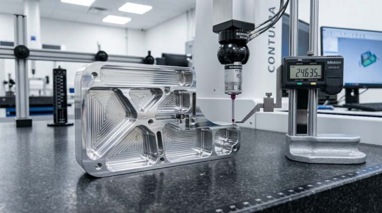
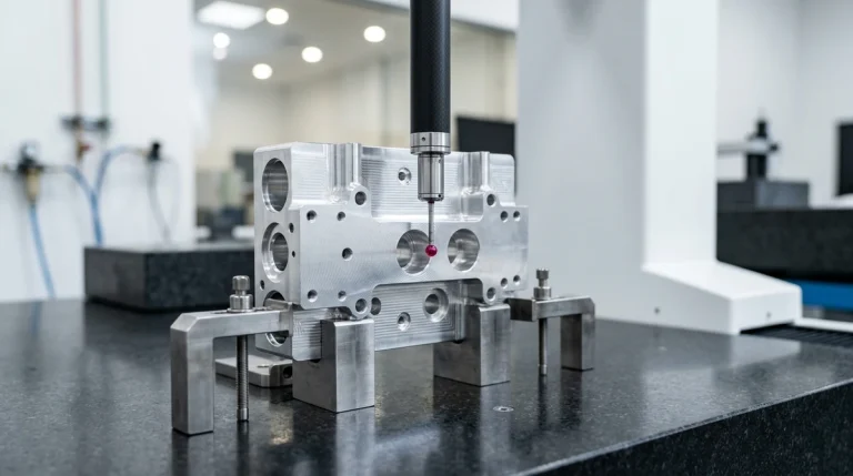
- Zeiss CMM Touch-Probe Metrology: Inspecting critical datum reference planes, bearing bores, and mounting hole centers to verify ISO 2768-mK and precision tolerances (±0.010 mm to ±0.020 mm).
- Neutral Salt Spray Fog Chambers: Continuous ASTM B117 testing up to 1,000 hours to ensure rugged outdoor survivability.
Hardware teams developing custom electronic assemblies can explore our comprehensive manufacturing capabilities across consumer electronics and appliance prototypes, examine our turnkey precision CNC machining services, and review our complete portfolio of industrial surface finishes.
Frequently Asked Questions
No. While bulk alumina has a lower thermal conductivity than raw aluminum, an electronic anodized film is only 15 to 25 microns thick. Its conductive resistance is virtually negligible (typically well under 0.01 K/W). Crucially, black anodizing raises radiative emissivity from 0.05 to about 0.90 or higher, increasing total passive heat dissipation by roughly 15% to 30% in fanless enclosures, depending on fin geometry.
Because anodic alumina is an electrical insulator, engineers employ three primary techniques: selective high-temperature silicone plug masking during plating, secondary CNC spot-facing milling to expose virgin conductive metal, or applying MIL-DTL-5541 Type II Class 3 conductive chemical conversion coating (chem film) across grounding bosses.
MIL-A-8625 Type II sulfuric anodizing with a thickness of 15 to 25 micrometers is optimal for consumer electronics. This thickness range provides rich dye color saturation, robust dielectric breakdown insulation up to 1,000 V, excellent scratch protection, and predictable dimensional growth.
Anodizing builds outward by approximately 50% of the coating thickness and penetrates inward by 50%. Outside diameters expand by the total coating thickness, and internal bores shrink by the total coating thickness. On 60-degree screw threads, outward growth reduces pitch diameter by approximately 4 times outward growth, requiring pre-plate oversize taps (6G/GH3) or silicone thread plugs.
Die-cast alloys like A380 and ADC12 contain 8% to 12% silicon and residual iron, which dissolve unevenly in acidic anodizing tanks, resulting in a dark, blotchy, or streaked grey surface finish. For cast electronics housings, we recommend MIL-DTL-5541 chemical conversion coating, powder coating, or electrostatic painting instead of decorative anodizing.
Request a Precision Electronic Enclosure & Anodizing DFM Review
Developing custom aluminum electronic chassis, heatsinks, or precision RF enclosures? AS Prototypes integrates multi-axis CNC machining, selective EMI masking, and verified MIL-A-8625 Type II/III anodizing. Our engineering team delivers comprehensive DFM feedback and precision dimensional verification within 24 hours.