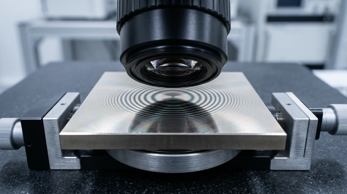
Across the frontiers of autonomous vehicle LiDAR assemblies, augmented reality (AR/VR) pancake optics, head-up displays (HUD), biomedical endoscopy, and high-energy laser collimators, optomechanical design has outgrown traditional planar mirrors and spherical glass geometries. Modern optical engineering mandates complex non-rotationally symmetric freeform surfaces, off-axis parabolic (OAP) reflectors, micro-structured Fresnel lens arrays, and continuous toroid light pipes. Fabricating these challenging geometries with sub-micron form fidelity and nanometer-level surface roughness cannot be achieved through conventional abrasive grinding and polishing. It demands ultra-precision optical precision machining, single point diamond turning (SPDT), and diamond micro-milling.
At AS Prototypes, we operate an ultra-precision diamond machining center and optical cleanroom metrology facility. Utilizing multi-axis diamond turning machines equipped with aerostatic spindles, hydrostatic slideways, slow/fast tool servos (STS/FTS), and robotic optical finishing, we manufacture custom prototypes and production inserts in optical polymers, non-ferrous alloys, and infrared crystals. Our manufacturing workflows deliver surface finishes down to Ra ≤ 1.5 nm and transmitted wavefront form accuracies within PV ≤ λ/4 at 632.8 nm.
Executive Summary & Engineering Takeaways (BLUF)
By: AS Prototypes Optical Engineering Team | Technical Review by: Senior Optomechanical Specialist
- Theoretical Kinematic Finish: In SPDT, theoretical surface roughness follows the cusp geometry Rmax = f2 / (8 · Rtool). Operating at feed rates of 1.0 to 2.5 μm/rev with a 1.5 mm nose radius monocrystalline diamond yields theoretical cusp heights of roughly 0.08 to 0.5 nm, achieving specular mirror finishes straight off the machine.
- Ductile-Regime Micro-Cutting: By restricting the uncut chip thickness below the critical depth of cut (dc ≈ 20 to 100 nm), brittle infrared crystals (Germanium, Silicon, ZnSe) undergo ductile plastic shear rather than micro-fracture, enabling crack-free specular finishes.
- Substrate Metallurgy & Chemical Constraints: Carbon steel, stainless steel, and titanium cannot be turned directly with diamond tools due to catastrophic catalytic graphitization wear (sp3 to sp2 phase transformation). Precision optical mold inserts must first be coated with 100 to 200 μm of amorphous high-phosphorus Electroless Nickel Plating (ENP, 10.5% to 13.0% P).
- Polymer Finishing Divergence: Chemical Vapor Polishing (CVP) with solvent vapors is strictly reserved for Polycarbonate (PC) and ABS, followed by mandatory thermal annealing (PC: 120°C to 125°C; ABS: 70°C to 80°C, below its Tg of about 105°C). CVP is strictly prohibited on PMMA (Acrylic), as solvent penetration induces micro-crazing and optical clouding; PMMA requires single-point diamond flycutting, diamond micro-milling, or robotic alumina slurry buffing.
- Metrology Hierarchy: Contact CMMs cannot verify optical surfaces. Full compliance verification requires non-contact Scanning White Light Interferometry (SWLI) for nanometer areal roughness (Sa, Sq) and 632.8 nm Laser Fizeau Interferometry for peak-to-valley (PV) wavefront error.
Quick Navigation: Optical Precision Machining Technical Architecture
- → 1. Micro-Cutting Mechanics & The Ductile Machining Regime
- → 2. Ultra-Precision Kinematics: SPDT, Flycutting & Multi-Axis Micro-Milling
- → 3. Diamond Tooling Metallurgy & The Graphitization Wear Mechanism
- → 4. Optical Substrate Selection & Material Properties Matrix
- → 5. Optical Finishing Protocols & Vapor Polishing Engineering Rules
- → 6. Design for Manufacturing (DFM) Rules for Diamond-Turned Optics
- → 7. Cleanroom Optical Metrology & Wavefront Phase Error Verification
- → 8. Engineering FAQ: Optical Precision Machining & Diamond Turning
1. Micro-Cutting Mechanics & The Ductile Machining Regime
In standard metal machining, chip removal operates via bulk plastic deformation along primary and secondary shear zones, where cutting depth significantly exceeds the tool edge radius. In contrast, optical precision machining functions in an extreme micro-mechanical domain where the depth of cut is often smaller than the natural crystalline grain boundaries of the workpiece and approaches the nanometer radius of the cutting edge.
For brittle optical crystals (such as single-crystal Germanium and Silicon) and optical polymers, executing crack-free specular cuts requires operating strictly within the ductile machining regime. Under extreme hydrostatic compressive stress concentrated directly beneath an atomically sharp diamond tool edge, the crystal lattice undergoes a localized high-pressure phase transformation (HPPT). This temporary amorphous metallic phase permits continuous plastic chip extrusion without initiating micro-crack propagation or sub-surface fracture.
The transition between brittle fracture and ductile shear is governed by the critical depth of cut (dc), expressed as:
dc ≈ 0.15 · (E / H) · (K1c / H)2
Where E represents Young’s modulus, H is the material’s micro-hardness, and K1c is the fracture toughness. For semiconductor-grade Germanium, the critical depth of cut sits near 40 to 80 nm. Exceeding this threshold causes brittle micro-chipping, resulting in subsurface scattering centers that degrade laser transmission. Keeping the uncut chip thickness strictly below dc produces continuous, ribbon-like ductile chips that reveal a pristine optical surface.
For ductile non-ferrous metals and amorphous polymers, the achievable surface texture in single point diamond turning is governed by kinematic tool-feed geometry. The theoretical peak-to-valley cusp height (Rmax) generated by overlapping tool nose arcs is given by:
Rmax ≈ f2 / (8 · Rtool) | Ra ≈ Rmax / 4 ≈ f2 / (32 · Rtool)
Where f is the cross-feed rate per workpiece revolution and Rtool is the controlled radius of the monocrystalline diamond nose. For example, programming a finishing pass with a tool radius of Rtool = 1.50 mm (0.059 in) at an ultra-fine cross-feed of f = 1.5 μm/rev (0.0015 mm/rev) calculates a theoretical cusp height of:
Rmax = (0.0015 mm)2 / (8 · 1.50 mm) = 2.25 × 10⁻⁶ / 12 mm = 0.0000001875 mm = 0.1875 nm
In shop-floor reality, achievable optical finishes are bounded not by tool geometry, but by secondary machine dynamics: spindle asynchronous error motion, building vibration, coolant mist pressure variations, and material grain boundaries. However, by strictly optimizing cutting parameters, our surface finishing protocols reliably achieve areal roughness values between Ra 1.0 nm and Ra 2.5 nm on optical aluminum, copper, and acrylic substrates.
2. Ultra-Precision Kinematics: SPDT, Flycutting & Multi-Axis Micro-Milling
Executing nanometer-level diamond machining requires machine tool structural stiffness and thermal loop stability that standard CNC machine centers cannot provide. Conventional ball screw drives and mechanical roller bearings generate micro-chatter and pitch ripple measured in microns—vastly exceeding the 400 nm to 700 nm wavelengths of visible light.
AS Prototypes deploys specialized multi-axis ultra-precision optical machining centers built upon massive natural granite machine bases (exceeding 3,000 kg). These platforms utilize passive and active dual-chamber pneumatic vibration isolation mounts with natural frequencies below 1.8 Hz, completely decoupling the cutting zone from ambient floor disturbances. Linear axes ride on liquid-cooled, non-contact aerostatic or hydrostatic guideways powered by ironless linear motors, eliminating mechanical backlash and cogging torque. Optical position feedback is captured via laser holographic glass scales with dynamic feedback interpolations down to 0.016 nm (16 picometers).
Workpiece spindles utilize pressurized aerostatic air bearings with radial and axial asynchronous runout held strictly below 15 nm (0.015 μm) TIR. Spindle drive motors are brushless DC direct-drive units equipped with internal liquid cooling to prevent motor winding heat from conducting into the air spindle shaft.
Before launching high-precision optical turning cycles, our optomechanical engineers select among three primary kinematic cutting modalities tailored to the optical component’s geometric symmetry, combining advanced CNC turning kinematics with specialized diamond toolpaths:
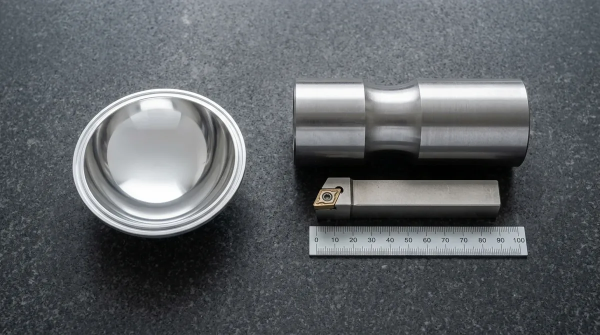
1. Single Point Diamond Turning (SPDT)
SPDT is the premier technique for rotationally symmetric optical geometries, including flat plano mirrors, standard spherical lenses, high-numerical-aperture (NA) aspheric elements, and off-axis parabolic (OAP) mirrors mounted in parent-mandrel fixtures. The substrate is secured to an air-bearing vacuum chuck rotating at 1,500 to 4,000 RPM, while the monocrystalline diamond tool moves along coordinated X and Z linear axes.
The diamond tool tip traces the mathematical profile of the aspheric optical sag equation, typically defined by the standard Even Asphere polynomial equation:
z(r) = (c · r2) / [1 + √(1 – (1 + k) · c2 · r2)] + ∑ A2i · r2i
Where c is the base surface curvature (1/R), k is the conic constant (hyperbolic, parabolic, or elliptical), and A2i represents higher-order even polynomial coefficients (4th, 6th, 8th, 10th order). SPDT produces finished optical lenses directly off the machine without introducing geometric roll-off at the edges.
2. Ultra-Precision Diamond Flycutting
For large-aperture plano optics, polygon scanning mirrors for laser imaging, and multi-faceted prism assemblies, diamond flycutting delivers superior surface flatness. The optical workpiece remains stationary or translates linearly on a horizontal traverse slide, while one or more natural diamond tools mounted on an offset rotating flycutter disc (typically 150 to 300 mm diameter) spin at 2,000 to 6,000 RPM across the part.
Because the cutting arc radius is exceptionally large relative to the optical aperture, flycutting produces parallel tool cusps with minimal mid-spatial frequency waviness. This kinematic arrangement regularly achieves plano wavefront flatness exceeding λ/10 PV (under 63 nm total form deviation) across apertures exceeding 150 mm.
3. Multi-Axis Diamond Micro-Milling & Tool Servos (STS / FTS)
When optical geometries depart from rotational symmetry—such as progressive ophthalmic lenses, automotive Head-Up Display (HUD) freeform combiners, continuous toroidal light pipes, or micro-lens arrays—conventional turning kinematics cannot maintain tool contact. We deploy two advanced kinematics:
- Fast Tool Servo (FTS): A high-bandwidth piezoelectric actuator drives the diamond tool along the Z-axis with high resonant frequencies (>1,000 Hz) but micro-stroke limits (typically 20 to 50 μm). FTS is ideal for micro-machining periodic Fresnel grooves, diffraction gratings, and micro-lens arrays directly onto curved substrates.
- Slow Tool Servo (STS): The workpiece spindle operates as a fully interpolated position-controlled rotary C-axis, coordinated dynamically with large-stroke X, Y, and Z linear axes. While restricted to lower rotational speeds (10 to 60 RPM), STS delivers full axial strokes exceeding 25 mm, permitting the direct diamond machining of radical freeform optical geometries and off-axis segments.
- Diamond Micro-Milling: Equipped with an auxiliary high-speed air-bearing milling spindle running at 60,000 to 100,000 RPM, specialized monocrystalline diamond ball endmills and micro-radius tools execute multi-axis contouring on polymer light guides, optical prisms, and fluidic diagnostic chips.
3. Diamond Tooling Metallurgy & The Graphitization Wear Mechanism
The cutting tool is the critical physical interface in optical precision machining. High-precision metalworking commonly utilizes carbide or polycrystalline diamond (PCD) inserts. However, PCD consists of randomly oriented diamond micro-grains bonded with cobalt solvent-catalysts, exhibiting edge roughness of 2 to 5 μm—vastly coarser than the desired optical finish. Ultra-precision machining relies strictly on monocrystalline natural or synthetic (HPHT / CVD) single-crystal diamonds.
Crystal Orientation and Atomic Sharpness
Single-crystal diamond possesses no internal grain boundaries. Specialist lapidaries orient the diamond along specific crystallographic planes—predominantly the {100} or {110} planes on the tool rake and clearance faces. These orientations provide maximum resistance to micro-chipping, highest cleavage resistance, and superior abrasive wear resistance.
Through specialized chemical-mechanical and ion-beam polishing, the cutting edge of a single-crystal diamond tool can be sharpened to an atomic edge radius of ρ ≤ 20 to 50 nm. This sharpness enables stable chip formation at nanometer depths of cut, ensuring true ductile shearing without plowing or smearing the substrate.
Thermal Conductivity & The High-Pressure Shear Zone
Monocrystalline diamond exhibits an extraordinary thermal conductivity exceeding 2,000 W/(m·K)—more than five times that of pure copper and twenty times that of tungsten carbide. During high-speed SPDT of optical polymers, cutting friction creates localized heat that could soften or melt the polymer. The high thermal conductivity of diamond rapidly pulls heat away from the micro-shear zone into the tool shank, maintaining substrate temperature below its glass transition temperature (Tg).
The Iron-Carbon Affinity: The Graphitization Wear Catastrophe
Despite its extraordinary hardness (10 Mohs / ~10,000 Vickers), diamond cannot be used to turn ferrous alloys (carbon steel, tool steel, stainless steel) or titanium under conventional conditions. This represents an unyielding metallurgical barrier:
Diamond is a metastable allotrope of pure carbon at atmospheric pressure, possessing a tetrahedral sp3 covalent crystal lattice. Under the high contact pressures (often exceeding 2 to 5 GPa) and elevated flash temperatures generated at the tool-chip interface, iron (Fe), nickel (Ni), cobalt (Co), and titanium (Ti) act as aggressive catalytic agents. The transition metals absorb carbon atoms into their empty d-electron orbitals, catalyzing an immediate transformation of the sp3 diamond lattice into planar sp2 graphite.
Simultaneously, carbon diffuses rapidly into the iron crystal lattice via solid-state interstitial diffusion. Under continuous turning of tool steel, a pristine monocrystalline diamond tool suffers catastrophic crater wear and edge recession exceeding 10 μm within minutes, destroying its cutting geometry and tearing the workpiece surface.
The Engineering Solution: High-Phosphorus Electroless Nickel Plating (ENP)
To produce steel-backed optical injection mold inserts, optomechanical engineers must decouple the diamond tool from catalytic iron atoms. This is achieved by depositing an intermediate layer of high-phosphorus Electroless Nickel Plating (ENP):
- Chemical Composition: We utilize an autocatalytic chemical nickel bath formulated to deposit 10.5% to 13.0% elemental Phosphorus by weight. At this specific composition, the nickel deposit exhibits an entirely amorphous (glassy, non-crystalline) microstructure with zero grain boundaries.
- Plating Thickness & Stress Relief: The pre-machined tool steel (such as 4140, P20, or Stavax ESR) is plated with 100 to 200 μm of high-phosphorus ENP. The core undergoes hydrogen embrittlement baking at 180°C to 200°C for 4 hours. Crucially, the temperature must remain below 240°C to prevent the precipitation of crystalline Ni3P intermetallic phases, which would degrade diamond turning quality for high-precision injection molding tooling.
- Machinability: Amorphous ENP does not react catalytically with diamond and exhibits no grain boundaries to deflect the cutting edge. Monocrystalline diamond tools cut amorphous ENP with exceptional ductile ribbon chips, regularly yielding optical mirror finishes with Ra ≤ 1.2 nm and minimal tool wear over hundreds of kilometers of cut distance.
4. Optical Substrate Selection & Material Properties Matrix
Selecting an optical substrate requires balancing optical performance (refractive index, dispersion, spectral transmission band, internal birefringence) against physical machinability, thermal expansion, and environmental durability. At AS Prototypes, our optical precision machining operations encompass four distinct material families: amorphous optical polymers, reflective non-ferrous metals, infrared crystalline semiconductors, and hard mold plating alloys.
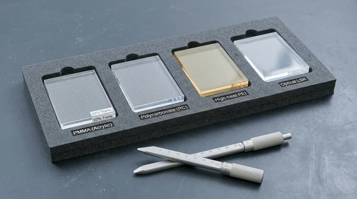
1. Optical Polymers (PMMA, PC, COP/COC, PEI)
- Optical Grade PMMA (Polymethyl Methacrylate): The standard for visible spectrum optics. PMMA offers 92% light transmission across 400 nm to 1,000 nm, an Abbe number of Vd = 58 (low chromatic dispersion), and exceptional SPDT machinability. PMMA shears with continuous, ductile ribbon chips, leaving specular, crystal-clear surfaces without post-polishing.
- Optical Polycarbonate (PC): Valued for extreme impact resistance and high refractive index (nd = 1.585). However, PC possesses a lower Abbe number (Vd = 30) resulting in higher dispersion. Its ductile elongation can cause edge burring during milling, requiring sharp diamond geometry and positive rake angles.
- Cyclic Olefin Polymers (COP / COC, e.g., Zeonex, TOPAS): Advanced cyclo-olefin resins designed for precision imaging optics. They feature high transmission (92%), near-zero moisture absorption (<0.01%), excellent dimensional stability up to 130°C, and near-zero stress birefringence (Δn < 10-6). COP is the premier choice for smartphone camera lens prototypes, biomedical flow cells, and NIR sensor windows.
- Optical Polyetherimide (PEI, Ultem 1010/1000): An amber-tinted high-heat amorphous thermoplastic with an exceptional glass transition temperature of Tg = 217°C. While absorbing visible blue light, PEI exhibits high transmission in the Near-Infrared band (850 nm to 1,550 nm), making it the primary choice for optical transceivers, LiDAR sensor covers, and harsh-environment thermal optics.
2. Reflective Optical Metals (Aluminum & Copper)
- Rapidly Solidified Aluminum (RSA-6061 / RSA-905): Standard commercial 6061-T6 contains coarse intermetallic silicon and magnesium silicide (Mg2Si) inclusions measuring 5 to 20 μm. When turned with diamond, these hard inclusions fracture and pull out of the soft aluminum matrix, creating microscopic pits that cause optical flare. To achieve laser-grade mirrors, we deploy melt-spun rapidly solidified aluminum alloys (RSA). RSA exhibits an ultra-fine microcrystalline microstructure (grain size <0.5 μm) with uniformly dispersed sub-micron phases, allowing direct SPDT finishing down to Ra ≤ 1.5 nm without micro-pitting.
- Oxygen-Free High Conductivity Copper (OFHC C10100): Delivers exceptional infrared reflectance (>99.2% at 10.6 μm) and superior thermal dissipation for high-power CO2 laser optics and synchrotron mirrors. Copper diamond-turns cleanly under light mineral oil mist, yielding specular surfaces with Ra ≤ 2.0 nm.
3. Infrared Crystal Semiconductors (Germanium & Silicon)
- Single-Crystal Germanium (Ge): The dominant substrate for Long-Wave Infrared (LWIR 8 to 12 μm) thermal imaging systems and FLIR lenses. Germanium provides an exceptionally high refractive index (n ≈ 4.00), enabling compact lens designs with minimal surface curvature. Using negative-rake monocrystalline diamond tools (-25° to -45°) under strictly controlled ductile regimes, Germanium turns to Ra ≤ 2.5 nm directly off the machine.
- Single-Crystal Silicon (Si): Widely deployed in Mid-Wave Infrared (MWIR 3 to 5 μm) sensors and laser mirrors due to its low density and high thermal conductivity. It requires precise ductile-regime cutting parameters to avoid brittle chipping.
| Substrate Material | Refractive Index (nd) | Abbe Number (Vd) | Primary Spectral Band | Diamond Machinability | Achievable Roughness (Ra) | Key Optical Application |
|---|---|---|---|---|---|---|
| Optical Grade PMMA | 1.491 | 58 (Low dispersion) | Visible & NIR (380 – 1,000 nm) | Exceptional; continuous ductile ribbon chips | ≤ 2.5 nm | AR/VR pancake lenses, HUD combiners, light pipes |
| Optical Polycarbonate (PC) | 1.585 | 30 (High dispersion) | Visible (400 – 800 nm) | High ductility; benefits from vapor polishing | ≤ 4.0 nm (Post-polish) | Impact-resistant sensor covers, automotive headlamps |
| Cyclic Olefin (Zeonex / TOPAS) | 1.530 | 56 (Low dispersion) | UV, Visible, NIR (300 – 1,100 nm) | Outstanding; zero water absorption, low stress | ≤ 2.0 nm | Micro-optics, medical diagnostic cells, mobile imaging |
| Optical PEI (Ultem 1010) | 1.630 – 1.680 | N/A (Amber visible) | Near-to-Mid IR (850 – 2,500 nm) | Good; high thermal stability (Tg 217°C) | ≤ 3.5 nm | High-temperature optical transceivers, LiDAR windows |
| Rapid-Solidified Aluminum (RSA-6061) | Reflective (>90%) | N/A (Mirror) | Visible, NIR, Far-IR | Superb; fine grain microstructure, zero pitting | ≤ 1.5 nm | Off-axis parabolic mirrors, telescope mirrors, flight payloads |
| High-Phos ENP on Tool Steel | Amorphous Tooling | N/A (Mold) | Tooling Substrate | Flawless; zero catalytic graphitization wear | ≤ 1.2 nm | Precision optical injection mold inserts, embossing shims |
| Monocrystalline Germanium (Ge) | ≈ 4.000 | N/A (Infrared) | LWIR (8.0 – 12.0 μm) | Brittle crystal; requires ductile regime parameters | ≤ 2.5 nm | Thermal imaging objectives, FLIR scopes, defense payloads |
5. Optical Finishing Protocols & Vapor Polishing Engineering Rules
While single point diamond turning produces pristine mirror finishes on rotationally symmetric surfaces, multi-axis diamond-milled light guides, complex prisms, and non-rotational optics often retain sub-micron tool cusps along complex corner blends. Bringing these surfaces to optical clarity requires tailored post-processing.
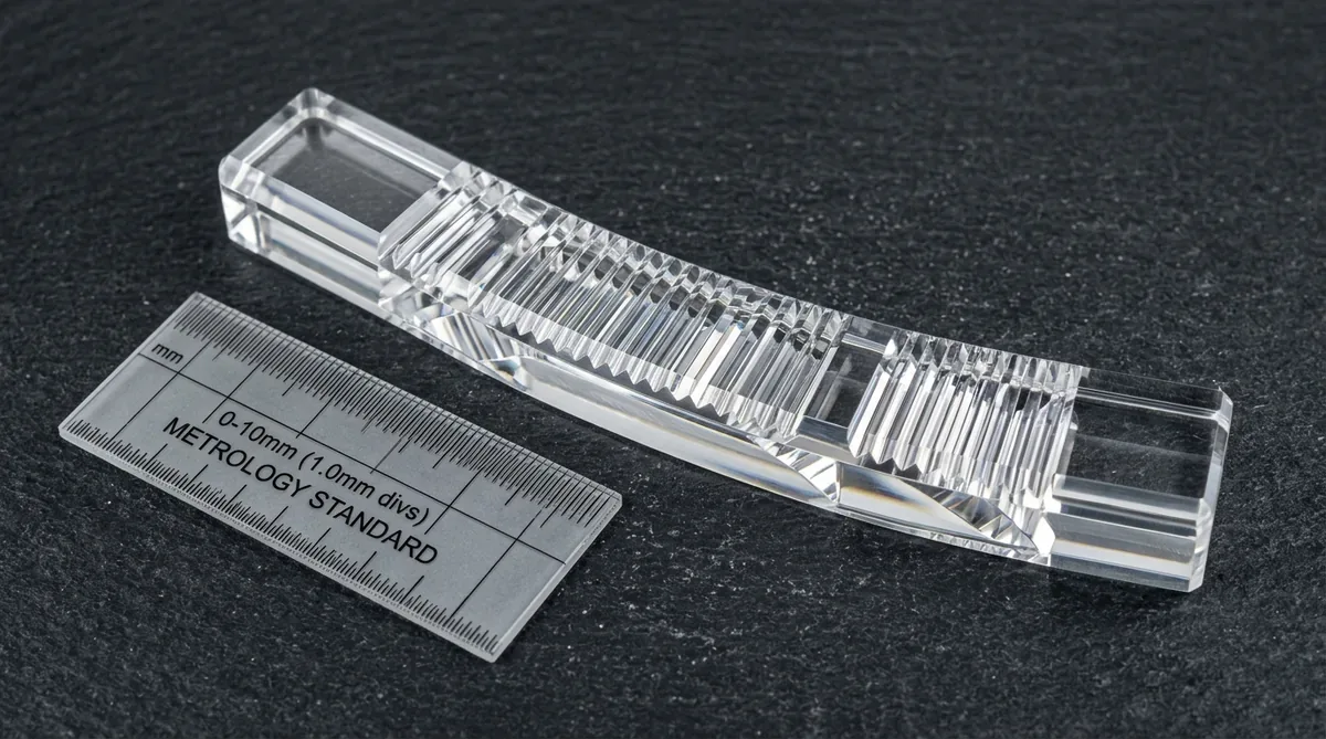
Crucial Engineering Distinction: The PMMA Solvent Crazing Prohibition
In prototyping shops, a frequent and costly engineering failure is attempting to smooth Acrylic (PMMA) using chemical solvent vapor polishing (CVP) with dichloromethane (methylene chloride). This practice is strictly prohibited in precision optics:
Polycarbonate (PC) responds exceptionally well to chemical vapor reflow because its high-molecular-weight bisphenol-A chains swell uniformly and reflow under mild solvent interaction. PMMA, however, possesses ester side chains that undergo rapid, non-uniform solvent absorption. The solvent creates extreme localized osmotic pressure gradients, triggering extensive subsurface micro-crazing (microscopic stress cracks). While the PMMA surface may appear shiny initially, the crazed microstructure causes severe internal Rayleigh and Mie scattering, clouding visible transmission and causing embrittlement. Under subsequent thermal cycling or mechanical load, crazed PMMA parts fail catastrophically.
PMMA Optical Finishing Protocols
To finish optical PMMA components without chemical degradation, AS Prototypes deploys non-chemical finishing workflows:
- Diamond Flycutting & Micro-Milling: Wherever geometry permits, the surface is cut directly to Ra ≤ 2.5 nm using single-crystal diamond tools, bypassing post-polishing entirely.
- Robotic Sub-Micron Slurry Buffing: For organic freeform contours and complex light pipes, components undergo automated multi-axis buffing utilizing ultra-soft cotton mops charged with high-purity, sub-micron colloidal alumina or cerium oxide slurries (particle diameter 0.05 to 0.10 μm). Surface removal is restricted to 0.5 to 1.0 μm to smooth tool cusps while preserving figure geometry.
- Precision Optical Flame Polishing: Restricted strictly to planar outer perimeter edges and non-imaging cylindrical profiles. A micro-orifice hydrogen-oxygen torch sweeps across the edge at high velocity, momentarily melting a surface layer under 2 μm thickness. Immediate thermal annealing follows.
Polycarbonate (PC) Chemical Vapor Polishing (CVP) & Post-Annealing
For complex polycarbonate light guides and automotive sensor housings, Chemical Vapor Polishing remains a powerful technique when executed with rigorous engineering controls:
- Vapor Chamber Exposure: The PC part is preheated to 50°C to prevent solvent condensation, then exposed to heated dichloromethane (CH2Cl2) azeotropic vapor for 5 to 15 seconds. Surface tension pulls microscopic machining cusps flat, yielding water-clear optical transparency.
- Mandatory Post-Vapor Thermal Annealing: Solvent reflow introduces significant localized tensile stress on the component surface. Unannealed vapor-polished PC parts will crack when exposed to cleaning agents, lubricants, or mechanical strain (Environmental Stress Cracking, ESC). Components must undergo a mandatory post-annealing bake in an air-circulating oven at 120°C to 125°C (just below PC’s Tg of 145°C) for 2 to 4 hours, followed by controlled slow cooling at ≤10°C/hour. This bake drives out residual solvent molecules and fully relaxes surface stresses.
Thin-Film Optical Cleanroom PVD Coatings
Following optical machining and surface stabilization, prototypes can receive high-vacuum Physical Vapor Deposition (PVD) optical thin-film coatings:
- Enhanced & Protected Aluminum: Thermally evaporated aluminum overcoated with dielectric layers (MgF2 or SiO2) providing >92% average reflectance across the visible spectrum (400 to 700 nm) while protecting the soft aluminum surface from oxidation and abrasion.
- Protected Gold: Sputtered pure gold with an adhesion-promoting titanium/chromium interlayer and protective overcoat, delivering >98.5% reflectance across Near-IR, Mid-IR, and Far-IR wavelengths (1 μm to 20 μm).
- Broadband Anti-Reflective (BBAR) Dielectric Stacks: Alternating nanometer-scale layers of high-index (TiO2, Ta2O5) and low-index (SiO2) dielectric materials engineered to eliminate surface Fresnel reflections, reducing single-surface reflectance from ~4% down to <0.5% per interface.
| Finishing Process | Compatible Substrates | Prohibited Substrates | Stock Removal / Depth | Achievable Finish | Mandatory Post-Treatment |
|---|---|---|---|---|---|
| Chemical Vapor Polishing (CVP) | Polycarbonate (PC), ABS | PMMA (Causes Crazing), Zeonex, Metals | 1.5 – 3.0 μm reflow layer | Ra ≤ 4.0 nm (Water-clear) | Thermal oven bake (PC: 120°C – 125°C; ABS: 70°C – 80°C) for 2 – 4 hours |
| Sub-Micron Slurry Buffing | PMMA, PC, Zeonex, Optical Silicone | Soft ductile metals (Embeds grit) | 0.5 – 1.0 μm abrasive removal | Ra ≤ 2.5 nm | Ultrasonic DI water wash with neutral surfactant |
| Direct Diamond Flycutting | PMMA, Zeonex, RSA Aluminum, OFHC Copper, ENP | Ferrous alloys, Titanium, Glass | Zero stock removal (Primary cut) | Ra ≤ 1.5 nm | Cleanroom solvent rinse & ionized nitrogen blow-off |
| PVD Thin-Film Vacuum Coating | All stabilized optical polymers & diamond-turned metals | Uncured / high-outgassing polymers | 100 nm – 2.5 μm film thickness | Reflectance >98% / AR <0.5% | Spectrophotometer transmission & adhesion tape test |
6. Design for Manufacturing (DFM) Rules for Diamond-Turned Optics
Designing components for ultra-precision diamond machining requires an optomechanical approach that differs substantially from standard CNC machining design guidelines. In diamond turning, tool clearance angles, internal vacuum mounting stress, and integrated datum alignment features directly determine whether optical tolerances can be met.
1. Tool Radius & Concave Surface Slope Clearance
When turning concave optical geometries (such as concave paraboloids, spherical mirrors, or deep reflectors), the monocrystalline diamond tool geometry imposes rigid geometric boundaries:
- Clearance Angle Interference: Diamond tools typically incorporate clearance angles between 6° and 12°. If the local slope angle of a concave optical sag approaches the tool clearance angle, the tool clearance flank rubs against the finished optical surface, causing catastrophic gouging and subsurface micro-cracking. Designers must verify that maximum surface slope does not exceed αmax ≤ Tool Clearance Angle – 3°. Standard tools with 6° to 12° clearance therefore suit gentle slopes only; steeper concave sags call for custom high-clearance diamond tools.
- Internal Concave Corner Radii: Sharp internal optical intersections cannot be turned. The minimum internal fillet radius must accommodate the diamond nose radius (typically R ≥ 0.5 to 1.5 mm). Attempting to force ultra-small corner radii requires micro-radius diamond tools (R = 0.05 mm), which exhibit fragile edges and dramatically increase cutting cycle times.
2. Datum Reference Alignment & Integrated Fiducial Features
In high-performance optomechanical assemblies, optical alignment (decentration, tilt, and focal plane positioning) often dominates system wavefront errors. Conventional secondary clamping introduces runout errors that degrade optical performance:
- Turned Datum A Reference Flange: Always design a precision planar mounting flange (Datum A) located directly adjacent to the optical aperture. In our SPDT setups, our machinists face this mounting datum in the identical spindle chucking setup as the optical mirror surface. This guarantees that axial runout and angular tilt between the mounting plane and optical optical axis remain below ≤ 2 μm (0.00008 in) and ≤ 10 μrad.
- Integrated Locating Pockets & Dowel Holes: Incorporate diamond-machined dowel pin bores or precision centering lands on the back or periphery of the component. Machining alignment features within the same machine coordinate system eliminates manual optical alignment during final assembly.
3. Spindle Center-Pip Elimination & Vacuum Clamping
- The Center-Pip Defect: In SPDT of convex or concave mirrors spanning across the spindle rotation center (r = 0), any microscopic misalignment between the diamond tool tip and the true spindle rotational axis results in a small uncut residual nub, known as a center-pip. While our machinists utilize micro-height optical sensors to set tool height within ≤0.2 μm, optomechanical designers should incorporate a small relief recess (Ø0.5 mm × 0.1 mm deep) at the non-functional optical center whenever optical path designs allow.
- Vacuum Chucking & Stress Birefringence: Traditional mechanical jaw chucking or perimeter set screws introduce non-uniform radial clamping forces. While a part may appear perfectly spherical while clamped, releasing it causes elastic springback that warps the surface into an astigmatic potato-chip profile (PV error >1.5 μm). Diamond turning mandates kinematic vacuum chucks, back-surface magnetic mounts, or integrated perimeter mounting tabs designed to isolate the active optical zone from clamping stresses.
| Geometric Parameter | Standard Engineering Class | Precision Optical Class | Ultra-Precision Laser Class | Critical DFM Design Consideration |
|---|---|---|---|---|
| Surface Roughness (Ra) | ≤ 5.0 nm | ≤ 2.5 nm | ≤ 1.2 – 1.5 nm | Substrate grain structure (use RSA aluminum or PMMA) |
| Form Accuracy (PV Error) | ≤ 0.50 μm (λ/1.3) | ≤ 0.25 μm (λ/2.5) | ≤ 0.10 μm (λ/6.3) | Thermal cleanroom stability & vacuum chuck kinematic isolation |
| Concave Slope Angle (α) | ≤ Clearance − 3° | ≤ Clearance − 3° | ≤ Clearance − 3° (High-Clearance Custom Tool) | Verify tool flank clearance to prevent heel rubbing; steep slopes require high-clearance custom diamond tools |
| Mechanical Center Runout | ≤ 5.0 μm | ≤ 2.0 μm | ≤ 0.8 μm | Single-chucking diamond facing of Datum A mounting bore |
| Optical Axis Tilt Error | ≤ 50 μrad (10 arcsec) | ≤ 20 μrad (4 arcsec) | ≤ 5 μrad (1 arcsec) | Incorporate integrated coplanar diamond-turned landing pads |
7. Cleanroom Optical Metrology & Wavefront Phase Error Verification
In precision optical manufacturing, a component is only as accurate as the metrology used to verify it. Standard mechanical inspection equipment (such as bridge CMMs equipped with ruby touch-trigger probes or standard dial indicators) cannot verify optical-grade parts: tactile probes exert millinewton contact forces that scratch delicate optical polymers, and their 0.5 to 1.0 μm measuring uncertainty exceeds the entire optical tolerance budget.
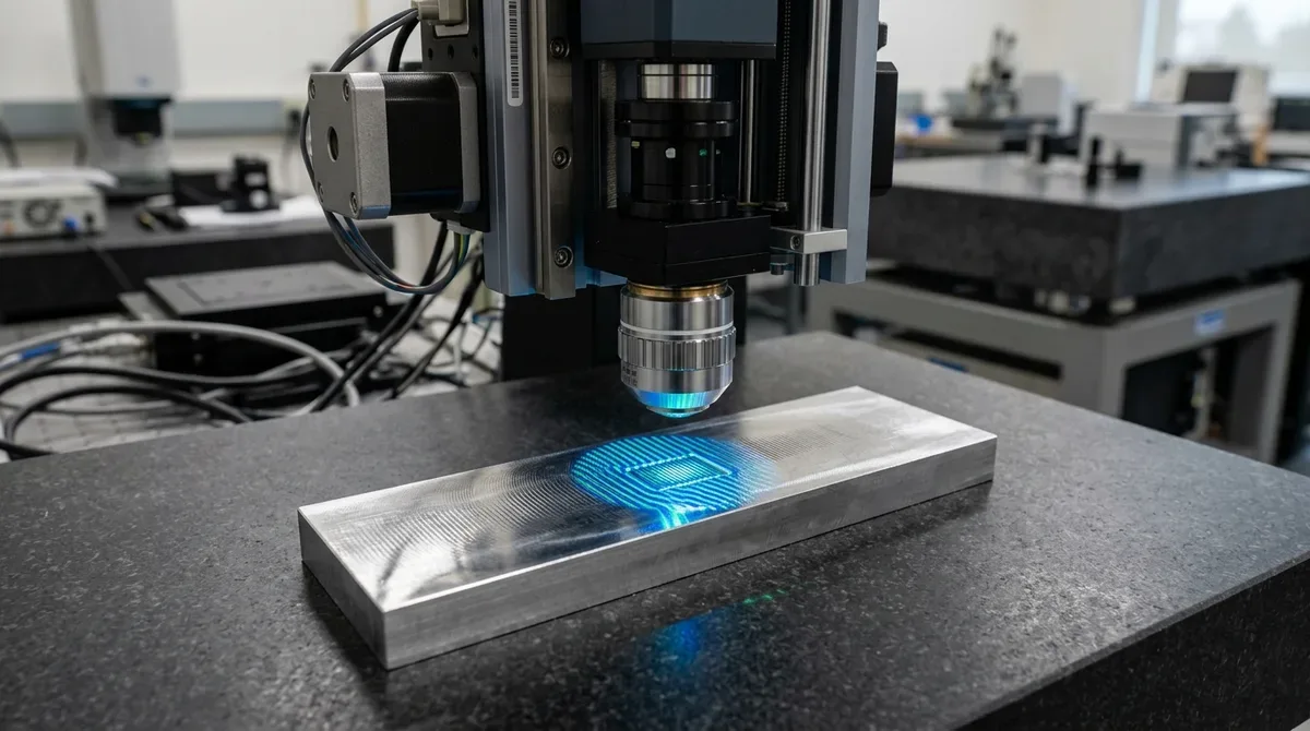
At AS Prototypes, all diamond-machined optics undergo 100% non-contact optical inspection in our Class 10,000 (ISO 7) temperature-controlled metrology laboratory (maintained at 20.0°C ± 0.2°C). We deploy a multi-tiered optical metrology suite:
1. Scanning White Light Interferometry (SWLI / CSI)
To quantify micro-roughness and optical flare scattering, we utilize coherence scanning white light interferometers (such as Zygo NewView systems). SWLI splits white light into a reference beam and a test beam reflected from the optical substrate. By scanning the interference fringe pattern vertically through focus, the instrument maps surface height with a vertical resolution under 0.05 nm (0.5 Angstroms) over a field of view ranging from 0.1 mm2 to multiple stitched square centimeters.
Rather than relying on single-line 2D roughness (Ra), SWLI calculates true 3D areal surface texture parameters in accordance with ISO 25178:
- Areal Roughness (Sa & Sq): Evaluates root-mean-square surface deviation across the entire functional aperture, confirming compliance with laser-grade scatter thresholds.
- Power Spectral Density (PSD): Deconstructs surface spatial frequencies into low-frequency form errors, mid-spatial frequency (MSF) waviness, and high-frequency micro-roughness. This ensures that diamond tool feed cusps do not generate diffractive halo artifacts in AR/VR and imaging applications.
2. Laser Fizeau Interferometry (Wavefront Verification)
For large plano mirrors, spherical optics, and transmitted optical assemblies, full-aperture 632.8 nm HeNe laser Fizeau interferometers evaluate macroscopic form accuracy. The interferometer compares the reflected or transmitted wavefront against a master reference transmission flat or transmission sphere master (λ/20 reference standard).
Fizeau interferometry outputs full-aperture wavefront deviation maps, calculating Peak-to-Valley (PV) error, RMS wavefront error, and mathematical Zernike polynomial decompositions. This allows our optomechanical engineers to isolate specific optical aberrations—such as spherical aberration, astigmatism, coma, and trefoil—and feed corrective toolpath offsets back into the diamond turning CNC controller (interferometric compensation loop).
3. High-Slope Aspheric & Freeform Profilometry
For steep aspheric and non-rotationally symmetric freeform optics where interferometric fringe density exceeds camera detector resolution, we deploy multi-wavelength heterodyne profilometers and sub-micron non-contact chromatic confocal sensors. These instruments track optical sag across apertures up to 250 mm with a coordinate measuring uncertainty below 15 nm, verifying true CAD mathematical profile alignment.
| Metrology System | Operating Principle | Vertical / Height Resolution | Primary Output Parameters | Target Inspection Task |
|---|---|---|---|---|
| Scanning White Light Interferometer (SWLI) | Broadband optical coherence scanning | < 0.05 nm (Sub-angstrom) | Sa, Sq, Sz, PSD frequency spectra | Nanometer micro-roughness, tool cusp height, diamond finish verification |
| Laser Fizeau Interferometer | 632.8 nm HeNe laser phase shifting | λ/1000 (≈ 0.6 nm) | PV Form Error, RMS wavefront, Zernike terms | Full-aperture transmitted and reflected wavefront error, lens aberrations |
| Chromatic Confocal 3D Profilometer | Wavelength-dispersed focus sensing | 5.0 nm | 3D sag point cloud, step height, thickness | Steep-angle freeform geometries, Fresnel lenses, micro-fluidic channels |
| Ultra-High Precision Tactile Profiler | Diamond stylus tracking (Form Talysurf) | 0.8 nm | 2D aspheric sag equation residual error | Long-range macro-aspheric profile curves up to 200 mm diameter |
8. Engineering FAQ: Optical Precision Machining & Diamond Turning
Diamond is composed of pure elemental carbon arranged in a tetrahedral sp3 covalent crystal lattice. At the extreme contact pressures and flash temperatures generated during cutting, iron, nickel, cobalt, and titanium act as active chemical catalysts. They absorb carbon into their electron orbitals, rapidly transforming the diamond cutting edge into planar sp2 graphite via catalytic graphitization. Simultaneously, carbon diffuses into the iron lattice, causing tool edge wear of over 10 microns within minutes. To diamond-turn steel optical mold cores, the steel substrate is plated with 100 to 200 microns of amorphous high-phosphorus Electroless Nickel Plating (ENP, 10.5% to 13.0% Phosphorus). Amorphous ENP does not react catalytically with diamond and turns smoothly to Ra under 1.2 nm.
No. Chemical solvent vapor polishing with dichloromethane (DCM) is strictly prohibited on PMMA components. PMMA contains ester functional groups that rapidly absorb solvent vapor, inducing localized osmotic swelling and severe micro-crazing (subsurface stress cracks). This causes internal optical scattering, hazing, and embrittlement. CVP is strictly reserved for Polycarbonate (PC) and ABS, followed by mandatory thermal annealing (PC: 120°C to 125°C; ABS: 70°C to 80°C, below its Tg of about 105°C). For PMMA optics, specular clarity must be achieved through direct single-point diamond flycutting, diamond micro-milling, or robotic multi-axis buffing with sub-micron alumina slurries.
While standard mechanical STEP and IGES solid models convey basic part boundaries and mounting interfaces, they approximate optical surfaces using polynomial NURBS patches that often introduce microscopic surface waviness. For precision freeform and aspheric optics, optical designers should supply analytical mathematical sag equations, polynomial coefficients (Even Asphere, Forbes Q-polynomials, or Zernike surface coefficients), or high-density native optical point-cloud matrices exported directly from optical design platforms like Zemax OpticStudio, Code V, or Synopsys LightTools.
Surface Roughness (Ra or Sa) measures high-frequency micro-irregularities (spatial wavelengths under 10 microns) caused by tool edge roughness and kinematic feed cusps; it dictates wide-angle optical scattering, flare, and stray light. In contrast, Peak-to-Valley (PV) form error evaluates low-frequency macroscopic deviations across the full optical aperture compared to the nominal mathematical design; it governs focal length fidelity, wavefront phase error, optical aberrations (such as spherical aberration and coma), and image resolution (MTF).
To eliminate assembly tilt and decentration, we machine precision Datum A mounting flanges and alignment pilot bores in the identical spindle setup and machine coordinate system as the active optical mirror. Because the optical aperture and the mechanical mounting interface are faced in a single continuous chucking operation, axial runout and angular tilt between the mounting plane and optical axis are held within 2 microns and 10 microradians, eliminating costly multi-axis optical alignment during assembly.
Bring Your Freeform Optical Prototypes to Specular Reality
From nanometer-smooth SPDT aspheres and AR/VR pancake lenses to diamond-machined optical mold inserts and freeform automotive HUD mirrors, AS Prototypes provides the multi-axis diamond machining agility and Zygo interferometric validation your optics demand. Receive detailed DFM feedback and an engineering review within 24 hours.
Request an Optical Machining DFM Review