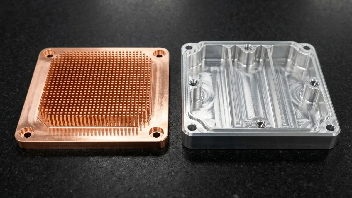
Mastering cnc machining for electronics is essential for hardware teams balancing tight dimensional tolerances, surface integrity, and scalable production economics. The relentless pace of hardware innovation—driven by high-density 5G infrastructure, edge artificial intelligence computing, IoT sensors, RF modules, and sleek handheld consumer devices—has pushed electronics packaging to microscopic thresholds. Modern electronic products demand unprecedented heat dissipation, hermetic sealing, electromagnetic compatibility (EMC), and millimeter-level packaging efficiency. To satisfy these non-negotiable physical constraints, precision CNC machining has become the cornerstone manufacturing methodology bridging rapid developmental prototyping and high-reliability series production.
Unlike injection molding or die casting, which require months of high-capital steel tooling fabrication, multi-axis CNC machining translates 3D CAD geometries directly into functional metal and polymer components within days. In this comprehensive engineering guide, our manufacturing team examines the core mechanical challenges, thermal and RF requirements, material selection matrix, and design-for-machinability (DFM) best practices for CNC machined electronics.
Executive Summary & Engineering Takeaways (BLUF)
- Thermal & EMI Performance: High-speed 3-axis and 4-axis CNC milling fabricates monolithic 6061-T6/6063-T6 aluminum and C10100/C11000 copper heat sinks, liquid-cooling cold plates, and multi-cavity RF waveguide enclosures that achieve >80 dB electromagnetic interference (EMI) attenuation.
- Tight PCB & Connector Alignment: Precision boring and multi-face indexing hold M1.6–M3 standoff thread true positions within ±0.015 mm (±0.0006″) and thermal interface mounting flatness within 0.025 mm per 100 mm (0.001″ per 4″) to minimize contact thermal resistance.
- Conductive vs. Dielectric Finishes: Combines MIL-DTL-5541 Type II (SurTec 650 / Alodine) trivalent chromate conversion or electroless nickel plating (ENP) on grounding flanges with selective masking on MIL-A-8625 Type II/III anodized exterior chassis walls.
- Insulating Engineering Polymers: Processes antistatic ESD-PEEK, PTFE (Teflon), Ultem 1000 (PEI), and G10/FR4 glass-epoxy for high-frequency RF radomes, semiconductor test sockets, and high-voltage busbar insulators with zero tooling investment.
Article Engineering Navigation
- 1. Why Modern Electronics Rely on Precision CNC Machining
- 2. Core CNC Machined Components in Electronics Hardware
- 3. Engineering Material Selection Guide for Electronics Machining
- 4. Surface Finishing and Post-Processing for Electronic Components
- 5. Design for Machinability (DFM) Guidelines for Electronic Enclosures
- 6. Quantitative Cold-Plate Thermal Resistance, RF Cavity Cutoff & Skin-Depth Physics
- 7. Technical Engineering FAQ
1. Why Modern Electronics Rely on Precision CNC Machining
The electronics industry operates under distinct mechanical and environmental stresses that differ fundamentally from structural machinery. CNC machining fulfills several mission-critical manufacturing objectives:
- tight tolerances (±0.015 mm / ±0.0006″) & Geometric Precision: High-density surface mount devices (SMD) and micro-BGA chips demand mounting bosses, alignment dowels, and connector cutouts held to positional tolerances of ±0.01 mm to ±0.005 mm to prevent solder joint fatigue and assembly misalignment.
- Electromagnetic Interference (EMI) & RF Isolation: High-frequency transceivers, phased-array radars, and wireless communication hardware require multi-cavity enclosures with milled labyrinth joints, conductive gasket channels, and unbroken metallic walls that prevent electromagnetic cross-talk and signal leakage.
- Direct Integration of Advanced Thermal Management: High-power semiconductors generate intense localized heat fluxes exceeding 100 W/cm². CNC milling allows engineers to sculpt micro pin-fin geometries, vapor chamber cavities, and liquid cooling channels directly into high-conductivity copper and aluminum blocks.
- Structural Rigidity and Drop Protection: Portable electronics (tablets, ruggedized smartphones, action cameras, wearable displays) rely on CNC machined unibody frames to protect delicate display panels and multilayer PCBs against torsional bending, impact shock, and environmental ingress.
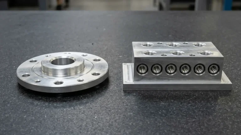
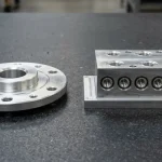
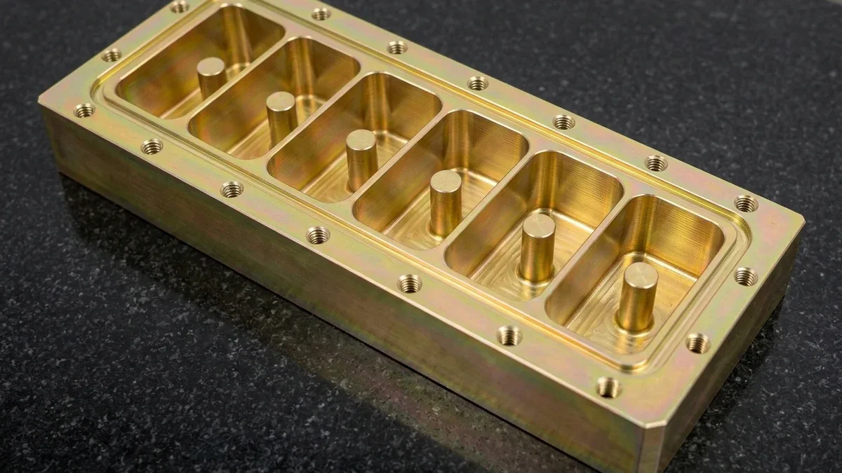
For high-frequency communications hardware, Figure 1 presents a CNC-milled 6061-T6 aluminum RF microwave waveguide cavity filter block finished with golden iridescent chromate conversion coating per MIL-DTL-5541 Type II. Precision-milled internal resonator posts and thin partition walls preserve low surface contact resistance and strict electromagnetic isolation.
2. Core CNC Machined Components in Electronics Hardware
Across both professional industrial electronics and sleek consumer devices, CNC machining produces components across four primary functional domains:
1. Structural Enclosures and Unibody Chassis
From aerospace-grade avionics packaging to premium laptops and wearable housings, CNC machined housings provide the primary structural skeleton. Advanced 5-axis milling machines contour internal rib patterns, integral threaded standoffs, battery cradles, and micro-perforated acoustic speaker grilles from solid monolithic billets of aluminum or magnesium-lithium alloys, eliminating the structural weak points inherent to multi-piece assemblies.
2. Active and Passive Heat Sinks
While standard low-power chips often utilize stamped or extruded aluminum heatsinks, high-density computing platforms, power amplifiers, and laser diodes demand custom CNC-sculpted heatsinks. High-speed CNC routers and mills produce ultra-thin cooling fins (with thicknesses down to 0.4 mm and aspect ratios up to 10:1), skewed airflow channels, and mirror-flat chip contact pads with surface flatness under 0.015 mm.
3. RF / Microwave Shielding Cavities
Telecommunications hardware, satellite transponders, and millimeter-wave radar modules require precision-milled aluminum shielding cavities. These parts feature intricate internal partitions separating individual RF amplifier stages. Machining these cavities from 6061-T651 aluminum prevents cavity warpage and ensures tight mechanical interlocks that attenuate spurious radiofrequency emissions by more than 80 dB.
4. Test Sockets, IC Burn-In Nests, and Semiconductor Handling Tools
During the validation of semiconductor packages and printed circuit assemblies, automated testing equipment utilizes custom CNC-machined test sockets and IC carrier nests. Fabricated from ultra-stable engineering plastics like PEEK, Torlon, or POM-C, these fixtures feature micro-drilled pogo-pin arrays with hole diameters as small as Ø0.25 mm and true position tolerances within ±0.008 mm.
3. Engineering Material Selection Guide for Electronics Machining
Selecting the optimal material for electronic hardware requires balancing electrical resistivity, thermal conductivity, mechanical machinability, weight, and post-machining surface treatment compatibility. The table below outlines the primary engineering materials deployed across our precision machining facilities:
| Material & Grade | Thermal & Electrical Properties | Machinability & Stability | Achievable Tolerance | Key Electronic Applications |
|---|---|---|---|---|
| Aluminum 6061-T651 | Thermal: ~167 W/m·K Good EMI shielding, non-magnetic | Excellent; stress-relieved stretching prevents pocket warpage | ±0.010 mm | Device unibody frames, RF shielding boxes, power inverter cold plates |
| Pure Copper (C10100 / C11000) | Thermal: ~390–400 W/m·K Electrical: 100% IACS | Moderate; gummy cutting behavior requires sharp carbide and MQL | ±0.015 mm | Micro-channel cold plates, CPU/GPU spreader blocks, high-current busbars |
| Brass (C36000 Free-Cutting) | Thermal: ~115 W/m·K Electrical: ~26–28% IACS | Outstanding; short, crisp chip formation, excellent thread strength | ±0.005 mm | SMA/BNC RF coaxial connectors, precision terminal pins, threaded standoffs |
| Stainless Steel (SUS304 / SUS316L) | Thermal: ~15–16 W/m·K Non-magnetic, superior sweat/salt resistance | Challenging; work hardening requires rigid toolpaths and high torque | ±0.012 mm | Smartwatch bezels, wearable sensor rings, ruggedized outdoor enclosures |
| PEEK (Polyetheretherketone) | Dielectric breakdown: ~20 kV/mm Continuous service up to 250°C | High; requires annealed stock to prevent internal stress deformation | ±0.010 mm | Semiconductor wafer carriers, high-frequency test sockets, high-voltage isolators |
| Delrin / POM-C (Polyacetal) | Volume resistivity: 1014 Ω·cm Low moisture absorption <0.2% | Superb; free-cutting, burr-free edges, low friction coefficient | ±0.015 mm | PCB assembly holding jigs, insulating spacers, sliding switch actuators |
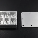
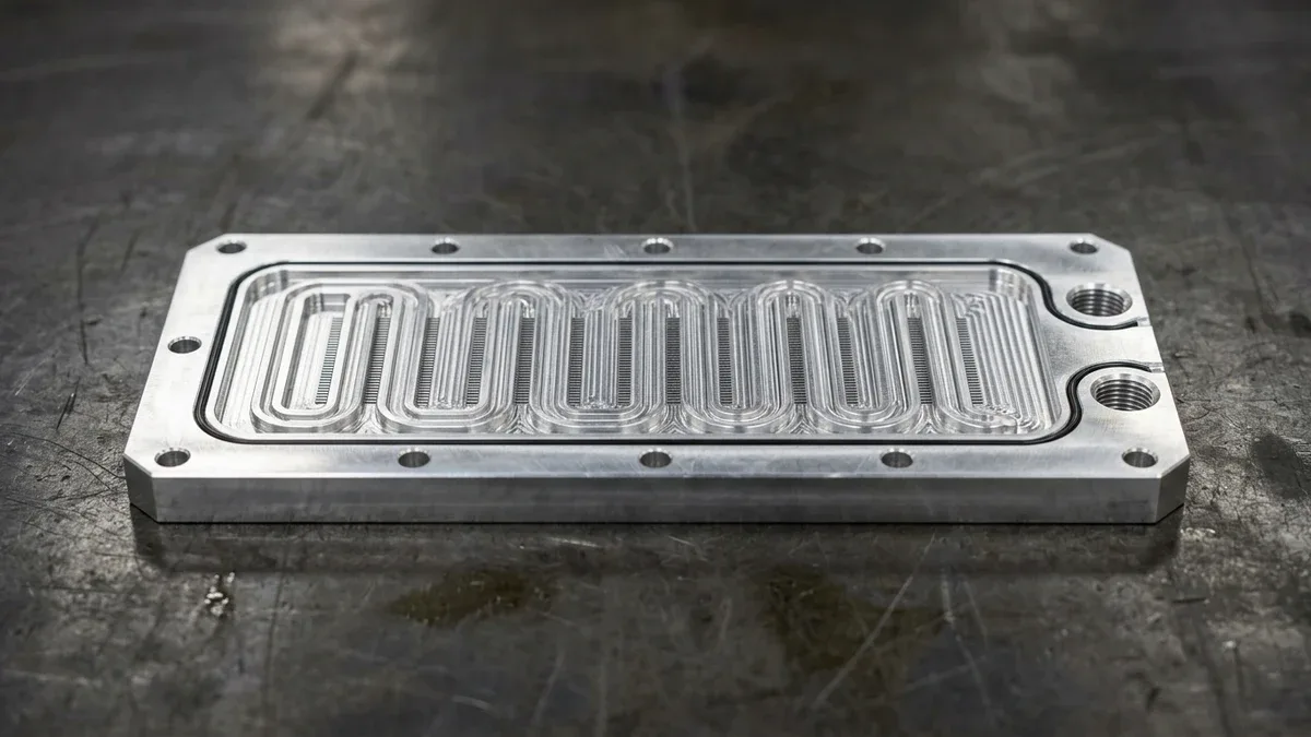
To manage high thermal flux in power electronics, Figure 2 displays a CNC-milled 6063-T6 aluminum liquid-cooling cold plate manifold featuring serpentine micro-fin fluid channels and a precision perimeter O-ring groove. Maintaining burr-free channel walls and flat sealing lands ensures leak-proof thermal transfer under continuous coolant pressure.
4. Surface Finishing and Post-Processing for Electronic Components
For electronic hardware, surface finishing is not purely cosmetic; it defines corrosion resistance, thermal emissivity, dielectric breakdown behavior, and electrical grounding conductivity. At AS Prototypes, we execute specialized surface finishing operations engineered for electronic environments:
- Type II & Type III (Hardcoat) Anodizing: An electrochemical oxidation that produces a durable, scratch-resistant oxide film (10–50 μm) on aluminum. The anodized layer acts as an electrical insulator with high breakdown voltage while significantly enhancing radiative thermal emissivity.
- Selective Conductive Masking & Chemical Conversion (Chromate / Alodine): When an enclosure exterior requires colored decorative anodizing but the internal mounting bosses must maintain grounding and EMI contact continuity, precision silicone plugs or chemical masking tapes preserve raw conductive surfaces treated with MIL-DTL-5541 chromate conversion.
- Electroless Nickel Plating (ENP): Provides a uniform, hard barrier coating over copper, brass, and aluminum cavities. ENP ensures exceptional solderability, low electrical contact resistance, and prevents galvanic oxidation in corrosive outdoor or marine operating environments.
- Ceramic & Glass Bead Blasting: Deployed prior to anodizing, automated bead blasting removes directional micro-tool marks and creates a velvet-like, non-directional matte texture (Ra 0.8–1.6 μm) that resists fingerprint staining on premium handheld consumer electronics.
- Laser Micro-Engraving: High-precision fiber laser markers permanently engrave regulatory compliance symbols (CE, FCC, RoHS), microscopic 2D DataMatrix QR codes, pin-out schematics, and serialized product numbers directly onto anodized or plated surfaces without altering part dimensions.
5. Design for Machinability (DFM) Guidelines for Electronic Enclosures
Optimizing your CAD model for CNC machining drastically cuts cycle times, prevents tool deflection, and guarantees part repeatability. Consider these fundamental DFM rules before submitting final production files:
- Maintain Realistic Internal Corner Radii: Micro-end mills with cutting diameters below 1.0 mm suffer from extreme deflection and breakage risk. Where pocket depth exceeds 10 mm, design corner radii to at least R1.5 mm (accommodating a Ø3.0 mm roughing tool), or incorporate relief “dog-bone” cuts where circuit board corners must seat flush.
- Avoid Overly Thin Wall Geometries: While consumer electronics demand extreme lightness, milling aluminum walls thinner than 0.6 mm (or plastics under 1.0 mm) induces severe vibrational chatter and dimensional drift during milling. Stiffening ribs should be added where ultra-thin sections are mandatory.
- Standardize Fastener Depths and Tapped Holes: Design blind tapped holes (M1.6, M2.0, M2.5) with thread depths limited to 2.5 to 3.0 times the nominal bolt diameter, providing at least 1.0 mm of drill point clearance beyond the full thread depth to prevent tap breakage in blind holes.
- Specify Grounding Contact Planes Clearly: When functional grounding is required between internal circuit modules and the metallic chassis, highlight these zones on 2D engineering drawings with specific GD&T flatness callouts (≤ 0.02 mm) to guide machining and masking operations.
By pairing early DFM analysis with advanced 3-, 4-, and precision CNC machining infrastructure, engineering teams can shave weeks off product development cycles while achieving flawless assembly fits. Explore our full spectrum of rapid manufacturing capabilities for smart devices and smart hardware across our dedicated consumer electronics and appliance solutions.
6. Quantitative Cold-Plate Thermal Resistance, RF Cavity Cutoff & Skin-Depth Physics
Interfacial Thermal Contact Resistance and Fly-Cut Flatness Mechanics
In high-heat-flux power electronics, AI accelerator cold plates, and SiC inverter baseplates, total junction-to-coolant thermal resistance (Rth,total) is dominated by the microscopic air gap between the semiconductor package and the CNC-machined metal pedestal. Because air has a thermal conductivity of only 0.026 W/(m·K) compared to 167 W/(m·K) for 6061-T651 aluminum and 398 W/(m·K) for C11000 copper, any surface bow forces Thermal Interface Material (TIM) bond lines to thicken.
• Conduction & Interface Thermal Resistance: Rth = (BLTTIM / (kTIM × A)) + (tbase / (kmetal × A)) [K/W]
• Rectangular RF Waveguide Dominant Cutoff Frequency: fc,TE10 = c / (2 × a) [Hz] (where a = internal cavity width, c = 3 × 10⁸ m/s)
• High-Frequency Conductor Skin Depth: δskin = √[ ρe / (π × f × μ0 × μr) ] [m] (≈ 0.66 μm in Cu at 10 GHz)
RF Shielding Cavity Waveguide Resonance and Partition Wall Milling
When machining multi-compartment RF and microwave amplifier housings operating between 6 GHz and 40 GHz, any internal cavity width (a) exceeding half a wavelength allows parasitic waveguide propagation across compartments. Furthermore, because electromagnetic currents above 10 GHz flow entirely within the outer 0.5–1.5 μm skin depth (δskin), internal cavity walls must be CNC-milled to Ra ≤ 0.8 μm (32 μin) and coated with high-conductivity silver or electroless nickel rather than thick insulating Type III anodize.
| Observed Defect / Symptom | Physical Root Cause | Quantitative Process Threshold | Corrective Shop-Floor Action | Inspection Verification Method |
|---|---|---|---|---|
| IGBT / processor thermal throttling on cold plate | Convex bow or coarse milling cusps increasing TIM bond-line thickness | Pedestal flatness > 0.030 mm per 100 mm or roughness Ra > 1.6 μm | Use stress-relieved 6061-T651 or C11000 plate and execute a single-pass diamond fly-cutting skim to Ra ≤ 0.4 μm | Zeiss CMM multi-point flatness scan and contact stylus profilometer |
| RF cross-talk and EMI leakage across lid-to-housing seam | Non-conductive Type II anodizing left on grounding flange or wide screw pitch | Contact resistance > 2.5 mΩ across seam or fastener spacing > λ/20 | Apply selective dual-finish (mask and Alodine/SurTec 650 chromate conversion on flange, Type II anodize on exterior) | 4-wire Kelvin milliohmmeter bond test and network analyzer shielding audit |
| Micro-drill breakage in PEEK / Torlon IC test sockets | Chip packing and frictional heat build-up in Ø0.20–0.40 mm pogo-pin arrays | Hole depth-to-diameter ratio L/D > 6:1 without peck clearing or air cooling | Run high-RPM (40,000 RPM) high-helix uncoated micro-carbide drills with 0.5×D peck cycles and chilled ionized air | Backlit 2.5D optical Vision Measurement System (VMS) true-position scan |
| Coolant weeping or braze porosity in liquid cold plates | Incomplete vacuum brazing or O-ring groove tool step-over marks | Helium leak rate > 1 × 10⁻⁷ mbar·L/s or O-ring groove Ra > 0.8 μm | Mill continuous contour O-ring glands with zero-stepover finishing passes and perform friction-stir welding or vacuum brazing | 10 bar hydrostatic pressure decay test and helium mass-spectrometer leak test |
Four-Step DFM Checklist for Electronic Enclosures and Heat Sinks
- Keep Pocket Corner Radii ≥ 1/6 of Cavity Depth: Avoid deep RF pockets with R0.5 mm vertical corners that force fragile long-reach micro-end mills; add dog-bone corner reliefs where rectangular PCBs must sit flush.
- Specify Dual-Finish Selective Masking for EMI Grounding: Call out conductive MIL-DTL-5541 / SurTec 650 or selective laser ablation on internal PCB ground pads while keeping protective Type II anodizing on outer cosmetic surfaces.
- Respect Extruded vs. Skived vs. CNC Fin Aspect Ratios: Limit straight CNC-milled cooling fin gaps to ≥ 1.5 mm (0.060 in) with height-to-gap ratios ≤ 6:1; for denser fin arrays, specify brazed or skived copper fin inserts.
- Isolate Tight True Position (±0.015 mm) to Board-to-Board Connectors: Apply standard ISO 2768-mK tolerances to outer chassis walls while anchoring blind-mate RF coaxial ports and alignment dowels to a single primary datum.
🔗 Related Electronics Hardware & Thermal Management Engineering Guides
7. Technical Engineering FAQ
CNC milling from wrought 6061-T651 plate delivers 167 W/m·K thermal conductivity and 90° vertical cavity walls, outperforming die-cast A380 at 96 W/m·K with 1.5° draft angles. Solid billet machining also eliminates internal porosity and tooling NRE, ensuring defect-free silver or gold RF plating.
MIL-A-8625 Type II and III anodic layers act as electrical insulators above 500 V breakdown, preventing direct grounding across anodized EMI grooves. Our shop applies conductive MIL-DTL-5541 or SurTec 650 conversion coating first, then masks EMI lands and PCB bosses before anodizing.
SiC IGBT and GPU cold plate pedestals require a surface roughness of Ra 0.4–0.8 µm and flatness within 0.025 mm per 100 mm to minimize TIM thermal resistance. Our shop holds these tolerances using stress-relieved 6061-T651 or C11000 copper stock finished with precision fly-cutting.
Standard aluminum electronics enclosures require a 0.8–1.2 mm minimum wall thickness and internal corner radii of ≥1.0 mm, or at least 1/6 of the cavity depth. This tool ratio prevents carbide end mill chatter, while RF waveguide filters use micro-milling spindles for 0.25 mm radii.
Ready to Validate Your CAD Design for Precision Manufacturing?
Upload your 3D CAD models (STEP, IGES, SolidWorks) and 2D engineering drawings for a comprehensive DFM engineering review and custom quotation from our in-house CNC machining and prototyping team.
Request a Custom DFM Review & Quote →