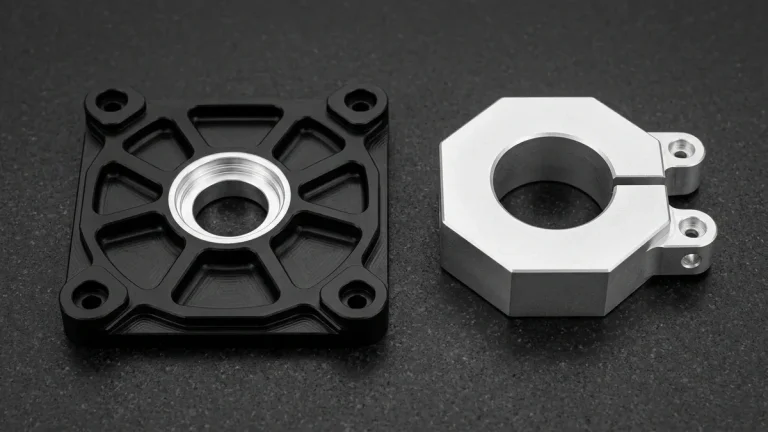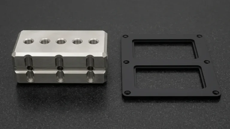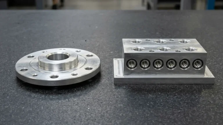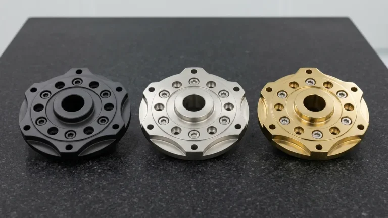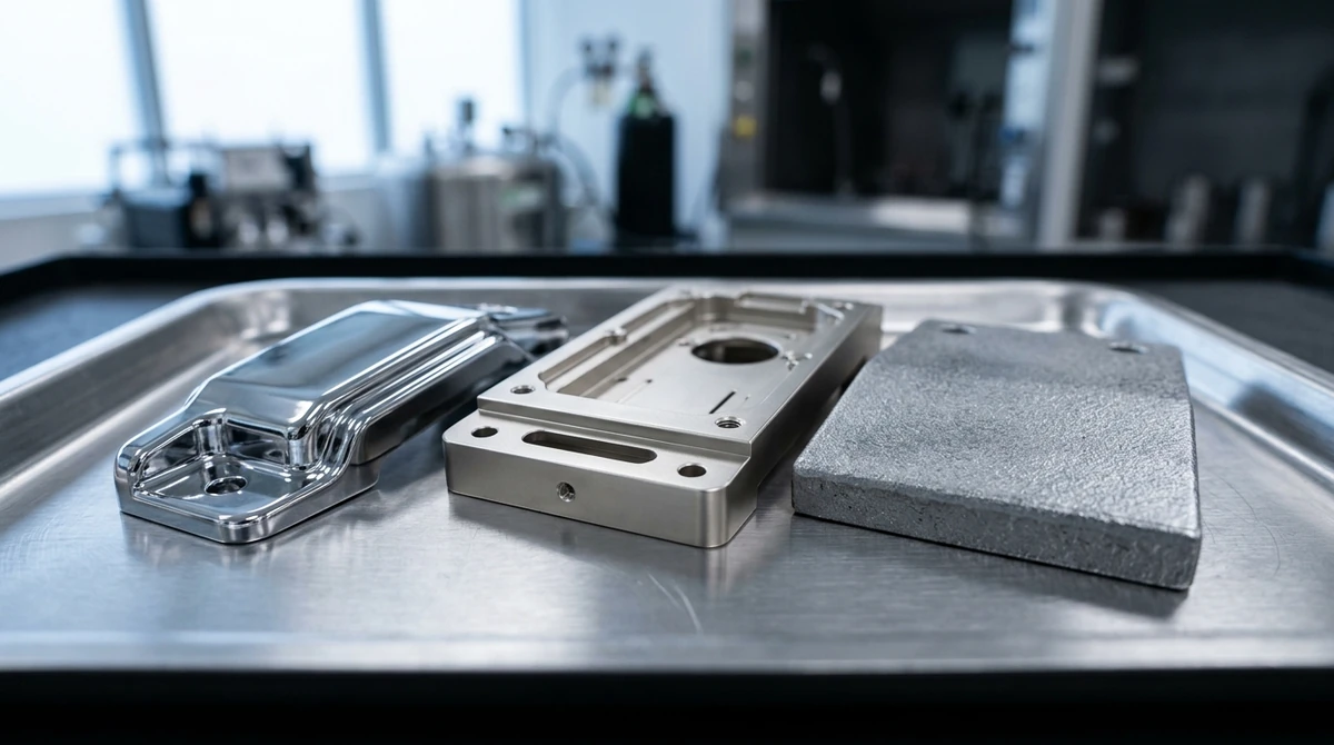
In contemporary engineering design, balancing the lightweight versatility and complex geometry of engineering polymers with the electrical, thermal, and barrier properties of structural metals is an essential objective. Making an entire component from solid stainless steel or brass adds excessive weight, machining time, and raw material cost.
Conversely, leaving polymer parts unshielded exposes sensitive electronics to electromagnetic interference (EMI) and environmental degradation. The technological solution that bridges these two material domains is metallization. In precision manufacturing, mastering what is metallization ensures repeatable dimensional stability and predictable production scaling.
At AS Prototypes, we provide turnkey manufacturing and surface finishing workflows—transforming CNC-machined plastics, 3D-printed resins, and vacuum cast polymers into highly functional, metallic-coated components. In this guide, our surface finishing engineers explain what metallization is, analyze the primary deposition processes (PVD, vacuum thermal evaporation, electroless plating, and electroplating), compare substrate compatibility, and provide practical Design for Manufacturing (DFM) rules.
- 1. What Is Metallization?
- 2. The 4 Primary Industrial Metallization Processes
- 3. Substrate Compatibility: Which Materials Can Be Metallized?
- 4. Comparative Matrix: Metallization Technologies
- 5. Engineering Case Study: AS Prototypes Medical Ultrasound Scanner Housing
- 6. Design for Manufacturability (DFM) Guidelines for Metallization
- 7. Technical Engineering FAQ
1. What Is Metallization?
Metallization is the process of depositing a thin, continuous layer of metal onto the surface of a non-metallic substrate (such as thermoplastics, thermosets, ceramics, composites, or glass) or another metallic substrate. The resulting hybrid component unites the structural benefits of the core material—such as low density, complex organic geometries, and low unit manufacturing costs—with the physical, functional, and aesthetic characteristics of a solid metal exterior.
Depending on the deposition technique and application, metallized coatings range from nanometer-thin films (0.05 μm) for optical mirrors to structural electroplated shells (25 to 50 μm) for automotive exterior trim.
Core Engineering Motivations for Metallization
- Electromagnetic and Radio Frequency Shielding (EMI/RFI): Lightweight polymer housings for aerospace avionics, medical diagnostic devices, and 5G telecommunications equipment require internal conductive metallic coatings (copper, nickel, or aluminum) to block external signal noise and contain internal high-frequency emissions.
- Electrical Conductivity and 3D Circuitry: Creating conductive traces directly on 3D polymer surfaces (Molded Interconnect Devices / 3D-MID) eliminates bulky wiring harnesses and planar printed circuit boards.
- Optical Reflectivity and Thermal Barrier: Deposition of pure vaporized aluminum provides up to 92% optical reflectivity for automotive headlamp reflectors, LiDAR optical sensors, and aerospace infrared thermal insulation shields.
- Wear, Hardness, and Chemical Barrier: Protecting soft plastic substrates against abrasive wear, UV radiation, hydrocarbon absorption, and moisture diffusion.
- Premium Aesthetics and Tactile Feel: Achieving an authentic “cool-to-the-touch” luxury metallic chrome, satin nickel, or brushed gold appearance on consumer electronic housings and automotive interior controls without the weight penalty of solid die-cast zinc or machined aluminum.
2. The 4 Primary Industrial Metallization Processes
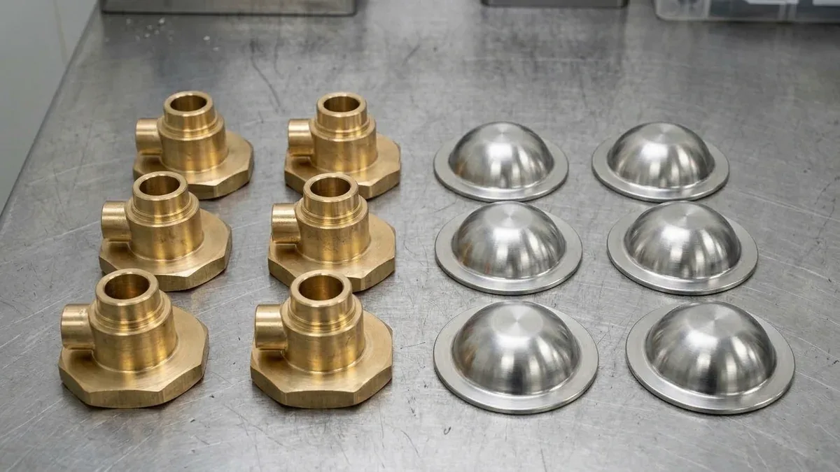
Selecting the optimal metallization route depends on coating thickness requirements, electrical conductivity needs, adhesion strength, part geometry, and production volume. The four dominant commercial methods are:
1. Physical Vapor Deposition (PVD)
Physical Vapor Deposition is an advanced vacuum coating process conducted inside a sealed chamber evacuated to high vacuum (10-3 to 10-6 mbar). The target metal (e.g., Titanium, Chromium, Zirconium, Gold, or Aluminum) is vaporized via magnetron sputtering or cathodic arc evaporation, ionizing the metal atoms into a high-energy plasma that condenses onto the substrate.
- Coating Thickness: 0.5 to 5.0 μm.
- Key Advantages: Ultra-pure deposition, exceptional atomic adhesion, environmentally benign (zero toxic chemical effluents), wide palette of decorative colors (TiN gold, TiCN gunmetal, AlCrN black, rainbow), and thin-film coating thickness control (1–5 μm).
- Best Suited For: High-end consumer electronics (smartwatch bezels, smartphone frames), optical components, medical surgical instruments, and decorative interior trim.
2. Vacuum Metallizing (Thermal Evaporation)
The standard workhorse for high-volume reflective plastic coatings. Parts are loaded onto a planetary carousel inside a vacuum chamber. Tungsten filaments loaded with high-purity aluminum clips or wire coils are electrically heated under high vacuum (10-4 Torr). The aluminum flashes instantly into a vapor cloud that condenses uniformly across all line-of-sight surfaces.
- Coating Thickness: 0.05 to 0.15 μm (50 to 150 nm).
- Layer Architecture: Because the vaporized aluminum layer is so micro-thin that it replicates microscopic substrate imperfections, a 3-layer system is mandatory:
- Basecoat: A UV-curable polyurethane lacquer applied to smooth out mold/machining toolmarks and seal polymer outgassing.
- Metal Vapor Layer: Pure evaporated aluminum (~0.1 μm) providing mirror-like reflectivity.
- Clear Topcoat: A hard UV-cured acrylic or polyurethane clearcoat to protect the fragile aluminum layer from oxidation, scratching, and moisture.
- Best Suited For: Automotive lighting reflectors, perfume bottle caps, toy components, and low-cost decorative bezels.
3. Electroless Plating (Chemical Autocatalytic Deposition)
Unlike electroplating, electroless plating requires no external electrical power. The substrate is immersed in an aqueous chemical bath containing dissolved metal salts (typically Nickel-Phosphorus or Copper) and a chemical reducing agent (such as sodium hypophosphite or formaldehyde). The chemical reaction is autocatalytic, driven by a catalytic seed layer (palladium-tin) previously deposited on the plastic surface.
- Coating Thickness: 1.0 to 25 μm.
- Key Advantages: 100% perfectly uniform coating thickness regardless of part complexity. Unlike electroplating—which builds up heavily on outer edges and starves deep blind holes—electroless plating coats internal cavities, cross-holes, and deep pocket ribs with identical thickness.
- Best Suited For: Internal EMI/RFI shielding for medical and aerospace electronics, complex electronic enclosures, and as the foundational conductive seed layer for Plating on Plastics (POP).
4. Electroplating on Plastics (POP)
Electroplating uses electrical current to reduce dissolved metal cations onto a conductive cathode. Because polymers are electrical insulators, parts must first receive a conductive foundation layer via electroless copper or nickel. Once conductive, the part enters standard electroplating baths to deposit robust layers of acid copper, semi-bright nickel, and a final decorative layer of trivalent or hexavalent chrome.
- Coating Thickness: 15 to 45 μm (total stack: ~20 μm copper + 15 μm nickel + 0.3 μm chrome).
- Key Advantages: Immense surface hardness, authentic cool metallic feel, rock-solid impact resistance, and maximum scratch resistance.
- Best Suited For: Automotive exterior grilles, emblem badging, door handles, plumbing fixtures, and heavy-use control knobs.
3. Substrate Compatibility: Which Materials Can Be Metallized?
Not all engineering materials bond equally well with metal layers. Polymer polarity, surface energy, and chemical etching susceptibility govern coating adhesion:
ABS (Acrylonitrile Butadiene Styrene)
The undisputed gold standard for plastic metallization. Chromic-sulfuric acid or plasma etching dissolves polybutadiene rubber nodules on the surface, leaving microscopic undercut anchor pits. Metal locks into these pits mechanically, delivering peel strengths exceeding 1.2–1.5 N/mm.
PC & PC/ABS Blends
Polycarbonate adds high thermal resistance (HDT > 130°C) and impact strength. Highly compatible with vacuum metallizing, PVD sputtering, and modified electroless plating. Essential for automotive lighting reflectors and telecom housings.
High-Performance Polymers (PEEK, Ultem PEI)
Aerospace and medical polymers require specialized oxygen/argon plasma pre-treatment to activate chemical bonding sites. Once activated, they accept high-adhesion PVD gold, titanium, or electroless nickel for extreme temperature environments (>200°C).
4. Comparative Matrix: Metallization Technologies
The following engineering matrix outlines the technical specifications, coating thicknesses, and primary applications across industrial metallizing processes:
| Process | Typical Thickness | Uniformity & Throwing Power | Common Deposition Metals | Primary Function | Relative Cost |
|---|---|---|---|---|---|
| Vacuum Thermal Evaporation | 0.05 – 0.15 μm | Line-of-sight (requires rotation) | Aluminum (99.99%) | Optical reflectors, decorative chrome look | Low (Economical Tier) |
| Physical Vapor Deposition (PVD) | 0.5 – 3.0 μm | High plasma distribution | TiN, ZrN, Cr, Gold, DLC | Wear resistance, premium color finishes | Moderate-High (Advanced Tier) |
| Electroless Chemical Plating | 2.0 – 15.0 μm | 100% Perfect Uniformity (all walls) | Electroless Nickel (Ni-P), Copper | EMI/RFI shielding, corrosion barriers | Moderate (Standard Tier) |
| Electroplating on Plastics (POP) | 15.0 – 45.0 μm | Current density dependent (heavy edges) | Cu + Ni + Hexavalent/Trivalent Cr | Heavy exterior durability, cold metal touch | High (Premium Tier) |
5. Engineering Case Study: AS Prototypes Medical Ultrasound Scanner Housing
The Challenge
A portable medical diagnostics manufacturer contracted AS Prototypes to prototype and serialize 500 units of an ergonomic handheld ultrasound scanner enclosure. The enclosure was CNC-machined from flame-retardant PC/ABS (UL 94-V0).
To comply with medical CE/FDA Class II electromagnetic compatibility (EMC) directives, the interior required a minimum attenuation of ≥65 dB shielding effectiveness across 100 MHz to 6 GHz. Externally, the client demanded a medical-grade satin silver finish resistant to harsh isopropyl alcohol hospital disinfectants.
AS Prototypes Engineering Solution
- Precision CNC Masking Fixture: Fabricated custom silicone elastomeric masking plugs to isolate external cosmetic surfaces from internal shielding baths.
- Internal Dual-Layer Electroless Plating:
- Primary Layer: 3.0 μm high-conductivity electroless copper (≤0.02 Ω/sq sheet resistance) for maximum electromagnetic attenuation.
- Protective Layer: 1.5 μm electroless nickel-phosphorus (8% P) to encapsulate the copper, preventing galvanic oxidation and corrosion.
- External PVD Sputtering: Placed components into our high-vacuum PVD sputtering chamber to deposit a 1.8 μm medical-grade Zirconium Nitride / Chromium satin silver film directly on the exterior casing.
The Results
- EMI Shielding Attenuation: Verified laboratory testing demonstrated 74 dB average attenuation across the target 6 GHz spectrum, completely passing EMC compliance.
- Chemical Resistance: Surpassed 5,000 continuous isopropyl alcohol (70% IPA) hospital wipe cycles with zero coating degradation, blistering, or flaking.
- Adhesion Integrity: Passed ASTM D3359 Cross-Hatch Tape Adhesion testing at Class 5B (100% adhesion retention).
6. Design for Manufacturability (DFM) Guidelines for Metallization
To avoid blistered coatings, poor adhesion, and dimensional out-of-tolerance rejects, incorporate these DFM rules into your CAD designs:
- Account for Coating Thickness in Tolerances: While vacuum metallizing (0.1 μm) has negligible dimensional impact, electroplating adds 30 to 45 μm per side (up to 0.090 mm on diameter!). Threaded holes, snap-fit tabs, and mating O-ring grooves must be modeled undersized/oversized accordingly, or explicitly masked on technical drawings.
- Avoid Razor-Sharp Edges (R ≥ 0.5 mm): In electroplating, high electrical current concentrates at sharp corners, causing excessive “dog-boning” metal buildup, nodules, and peeling. Generous edge radii promote uniform electrical field distribution.
- Incorporate Tooling Racking Points: Every part undergoing plating or PVD must be physically held on a conductive copper/titanium rack or carousel clamp. Design a non-visible internal tab, boss hole, or unplated rib to serve as the electrical contact and hanging point.
- Eliminate Blind Deep Holes: In vacuum metallizing and PVD, metal vapor travels strictly in straight lines (line-of-sight). Deep blind holes will receive zero coating. If internal coverage is mandatory, specify electroless chemical immersion plating instead.
At AS Prototypes, we provide end-to-end rapid prototyping and low-to-mid volume manufacturing under one roof: from high-speed 3-axis, 4-axis, and 5-axis CNC machining, rapid tooling injection molding, and vacuum casting, to high-vacuum PVD coating, vacuum thermal evaporation, and precision chemical plating lines.
7. Technical Engineering FAQ
PVD vacuum metallization vaporizes solid metal or ceramic targets in a high-vacuum chamber to deposit ultra-thin (0.2 to 5 µm), dense films such as TiN, CrN, or reflective aluminum. Electroless plating (such as electroless nickel or copper) uses autocatalytic chemical reduction in an aqueous bath to deposit a 100% uniform coating thickness across blind holes and complex internal cavities. Thermal spray propels molten metal droplets at high velocity to build thick (50 to 500 µm) structural wear or barrier coatings.
Plating-grade ABS contains uniformly dispersed polybutadiene rubber spheres within an acrylonitrile-styrene matrix. During chromic-sulfuric or environmentally friendly permanganate chemical etching, the butadiene spheres dissolve selectively, creating a microscopic network of 0.1–1.0 µm dovetail anchor pores that mechanically lock the electroless copper/nickel base layer with peel strengths exceeding 1.0 N/mm.
Polymer enclosures (PC, ABS, Ultem, PEEK) are electrically transparent to electromagnetic interference. Applying a dual-layer electroless copper (1.5 to 3.0 µm for high electrical conductivity) and electroless nickel topcoat (0.5 to 1.0 µm for corrosion protection and galvanic compatibility) provides 60 to 85 dB of EMI attenuation across 30 MHz to 10 GHz without the weight penalty of a solid metal housing.
For mirror-specular PVD or optical reflector metallization, the substrate must be diamond-turned or polished to Ra ≤ 0.02–0.05 µm because nanometer-thin vacuum films replicate underlying tool marks directly. For functional thermal spray or heavy electroplating, sharp external corners must be radiused to R ≥ 0.5–1.0 mm to prevent electrostatic current-density dog-boning and coating delamination.
Specify Verified Surface Finishes on Custom Precision Components
Ensure dimensional allowance control, thread masking accuracy, and MIL-A-8625 or ASTM surface compliance from raw billet machining through final finishing. Upload your 3D CAD models and 2D prints for a complete engineering DFM review.
Upload CAD & Drawings for Finishing DFM Review